15 Mar 00:25
J. Mater. Chem. A, 2017, 5,7118-7124
DOI: 10.1039/C7TA00698E, Paper
Sibai Li, Zhi Peng, Jiaxin Zheng, Feng Pan
CdTe is widely applied in thin film solar cells as a p-type layer, which is usually in contact with a metal back electrode.
The content of this RSS Feed (c) The Royal Society of Chemistry
15 Mar 00:13
by Stefan D. Oosterhout, Victoria Savikhin, Junxiang Zhang, Yadong Zhang, Mark A. Burgers, Seth R. Marder, Guillermo C. Bazan and Michael F. Toney

Chemistry of Materials
DOI: 10.1021/acs.chemmater.7b00067

14 Mar 01:13
J. Mater. Chem. A, 2017, 5,7516-7522
DOI: 10.1039/C6TA11012F, Paper
Markus W. Pfau, Andreas Kunzmann, Doris Segets, Wolfgang Peukert, Gordon G. Wallace, David L. Officer, Tim Clark, Ruben D. Costa, Dirk M. Guldi
A novel concept for constructing optimized ZnO-based photoanodes as integrative components of dye-sensitized solar cells (DSSCs) is realized by deploying differently sized nanoparticles ranging from 2 to 10 nm together with commercially available 20 nm nanoparticles.
The content of this RSS Feed (c) The Royal Society of Chemistry
11 Mar 01:24
by Miriam Más-Montoya, René A. J. Janssen
The performance of organic semiconductors in optoelectronic devices depends on the functional properties of the individual molecules and their mutual orientations when they are in the solid state. The effect of H- and J-aggregation on the photophysical properties and photovoltaic behavior of four electronically identical but structurally different thiophene–pyridine–diketopyrrolopyrrole molecules is studied. By introducing and changing the position of two hexyl side chains on the two peripheral thiophene units of these molecules, their aggregation in thin films between H-type and J-type is effectively tuned, as evidenced from the characteristics of optical absorption, fluorescence, and excited state lifetime. The two derivatives that assemble into J-type aggregates exhibit a significantly enhanced photovoltaic performance, up to an order of magnitude, compared to the two molecules that form H-type aggregates. The reasons for this remarkably different behavior are discussed.

The aggregation behavior of electronically identical thiophene–pyridine–diketopyrrolopyrrole molecules is modulated by introducing and modifying the position of two hexyl side chains on the peripheral thiophene rings. Improved photovoltaic performance is achieved for those molecules assembling into J-type aggregates in contrast to those forming H-aggregates as a result of a faster charge generation and a reduced bimolecular recombination.
11 Mar 01:23
by Fuwen Zhao, Shuixing Dai, Yang Wu, Qianqian Zhang, Jiayu Wang, Li Jiang, Qidan Ling, Zhixiang Wei, Wei Ma, Wei You, Chunru Wang, Xiaowei Zhan
A new fluorinated nonfullerene acceptor, ITIC-Th1, has been designed and synthesized by introducing fluorine (F) atoms onto the end-capping group 1,1-dicyanomethylene-3-indanone (IC). On the one hand, incorporation of F would improve intramolecular interaction, enhance the push–pull effect between the donor unit indacenodithieno[3,2-b]thiophene and the acceptor unit IC due to electron-withdrawing effect of F, and finally adjust energy levels and reduce bandgap, which is beneficial to light harvesting and enhancing short-circuit current density (JSC). On the other hand, incorporation of F would improve intermolecular interactions through C![[BOND]](http://onlinelibrarystatic.wiley.com/undisplayable_characters/00f8ff.gif) F···S, CF···H, and CF···π noncovalent interactions and enhance electron mobility, which is beneficial to enhancing JSC and fill factor. Indeed, the results show that fluorinated ITIC-Th1 exhibits redshifted absorption, smaller optical bandgap, and higher electron mobility than the nonfluorinated ITIC-Th. Furthermore, nonfullerene organic solar cells (OSCs) based on fluorinated ITIC-Th1 electron acceptor and a wide-bandgap polymer donor FTAZ based on benzodithiophene and benzotriazole exhibit power conversion efficiency (PCE) as high as 12.1%, significantly higher than that of nonfluorinated ITIC-Th (8.88%). The PCE of 12.1% is the highest in fullerene and nonfullerene-based single-junction binary-blend OSCs. Moreover, the OSCs based on FTAZ:ITIC-Th1 show much better efficiency and better stability than the control devices based on FTAZ:PC71BM (PCE = 5.22%).
F···S, CF···H, and CF···π noncovalent interactions and enhance electron mobility, which is beneficial to enhancing JSC and fill factor. Indeed, the results show that fluorinated ITIC-Th1 exhibits redshifted absorption, smaller optical bandgap, and higher electron mobility than the nonfluorinated ITIC-Th. Furthermore, nonfullerene organic solar cells (OSCs) based on fluorinated ITIC-Th1 electron acceptor and a wide-bandgap polymer donor FTAZ based on benzodithiophene and benzotriazole exhibit power conversion efficiency (PCE) as high as 12.1%, significantly higher than that of nonfluorinated ITIC-Th (8.88%). The PCE of 12.1% is the highest in fullerene and nonfullerene-based single-junction binary-blend OSCs. Moreover, the OSCs based on FTAZ:ITIC-Th1 show much better efficiency and better stability than the control devices based on FTAZ:PC71BM (PCE = 5.22%).

Single-junction binary-blend nonfullerene polymer solar cells based on fluorinated acceptor ITIC-Th1 afford power conversion efficiency of 12.1%, which is much higher than those of nonfluorinated ITIC-Th (8.88%) and PC71BM (5.22%) counterparts under the same condition. Moreover, the nonfullerene devices exhibit better thermal stability than the fullerene devices.
11 Mar 01:22
by Yasutaka Nagaoka, Katie Hills-Kimball, Rui Tan, Ruipeng Li, Zhongwu Wang, Ou Chen
Lead halide perovskites are promising materials for a range of applications owing to their unique crystal structure and optoelectronic properties. Understanding the relationship between the atomic/mesostructures and the associated properties of perovskite materials is crucial to their application performances. Herein, the detailed pressure processing of CsPbBr3 perovskite nanocube superlattices (NC-SLs) is reported for the first time. By using in situ synchrotron-based small/wide angle X-ray scattering and photoluminescence (PL) probes, the NC-SL structural transformations are correlated at both atomic and mesoscale levels with the band-gap evolution through a pressure cycle of 0 ![[LEFT RIGHT ARROW]](http://onlinelibrarystatic.wiley.com/undisplayable_characters/002194.gif) 17.5 GPa. After the pressurization, the individual CsPbBr3 NCs fuse into 2D nanoplatelets (NPLs) with a uniform thickness. The pressure-synthesized perovskite NPLs exhibit a single cubic crystal structure, a 1.6-fold enhanced photoluminescence quantum yield, and a longer emission lifetime than the starting NCs. This study demonstrates that pressure processing can serve as a novel approach for the rapid conversion of lead halide perovskites into structures with enhanced properties.
17.5 GPa. After the pressurization, the individual CsPbBr3 NCs fuse into 2D nanoplatelets (NPLs) with a uniform thickness. The pressure-synthesized perovskite NPLs exhibit a single cubic crystal structure, a 1.6-fold enhanced photoluminescence quantum yield, and a longer emission lifetime than the starting NCs. This study demonstrates that pressure processing can serve as a novel approach for the rapid conversion of lead halide perovskites into structures with enhanced properties.

Pressure processing of CsPbBr3 perovskite nanocube superlattices can generate 2D perovskite nanoplatelets that exhibit a single cubic crystal structure, a 1.6-fold enhanced photoluminescence quantum yield, and a longer emission lifetime than the starting nanocubes. Pressure processing can serve as a novel approach for the rapid conversion of lead halide perovskites into structures with enhanced structural and optical properties.
09 Mar 13:38
by Yun Hee Park, Inyoung Jeong, Seunghwan Bae, Hae Jung Son, Phillip Lee, Jinwoo Lee, Chul-Ho Lee, Min Jae Ko
Perovskite solar cells (PSCs) based on organic monovalent cation (methylammonium or formamidinium) have shown excellent optoelectronic properties with high efficiencies above 22%, threatening the status of silicon solar cells. However, critical issues of long-term stability have to be solved for commercialization. The severe weakness of the state-of-the-art PSCs against moisture originates mainly from the hygroscopic organic cations. Here, rubidium (Rb) is suggested as a promising candidate for an inorganic–organic mixed cation system to enhance moisture-tolerance and photovoltaic performances of formamidinium lead iodide (FAPbI3). Partial incorporation of Rb in FAPbI3 tunes the tolerance factor and stabilizes the photoactive perovskite structure. Phase conversion from hexagonal yellow FAPbI3 to trigonal black FAPbI3 becomes favored when Rb is introduced. The authors find that the absorbance and fluorescence lifetime of 5% Rb-incorporated FAPbI3 (Rb0.05FA0.95PbI3) are enhanced than bare FAPbI3. Rb0.05FA0.95PbI3-based PSCs exhibit a best power conversion efficiency of 17.16%, which is much higher than that of the FAPbI3 device (13.56%). Moreover, it is demonstrated that the Rb0.05FA0.95PbI3 film shows superior stability against high humidity (85%) and the full device made with the mixed perovskite exhibits remarkable long-term stability under ambient condition without encapsulation, retaining the high performance for 1000 h.

Partial substitution of inorganic rubidium cation (Rb+) for formamidinium lead iodide (FAPbI3) perovskite suppresses nonperovskite phase formation and increases fluorescence lifetime. Introduction of the smaller monovalent cation in FAPbI3 renders the perovskite more tolerant to high humidity. These lead to enhanced photovoltaic performances and long-term stability of perovskite solar cells based on Rb-mixed FAPbI3.
09 Mar 13:36
J. Mater. Chem. A, 2017, 5,6122-6130
DOI: 10.1039/C7TA00793K, Paper
Damien Joly, Maxime Godfroy, Laia Pelleja, Yann Kervella, Pascale Maldivi, Stephanie Narbey, Frederic Oswald, Emilio Palomares, Renaud Demadrille
We unraveled the role of alkyl substituents, usually employed as solubilizing groups for organic sensitizers, in the performances and the stability of photovoltaic devices.
The content of this RSS Feed (c) The Royal Society of Chemistry
09 Mar 13:36
J. Mater. Chem. A, 2017, 5,6638-6647
DOI: 10.1039/C7TA01467H, Paper
Serge Beaupre, Sepideh Shaker-Sepasgozar, Ahmed Najari, Mario Leclerc
New efficient D-A1-D-A2 random terpolymers for photovoltaic applications.
The content of this RSS Feed (c) The Royal Society of Chemistry
07 Mar 16:53
by Guiying Xu, Liang Shen, Chaohua Cui, Shanpeng Wen, Rongming Xue, Weijie Chen, Haiyang Chen, Jingwen Zhang, Hongkun Li, Yaowen Li, Yongfang Li
Polymer solar cells (PSCs) possess the unique features of semitransparency and coloration, which make them potential candidates for applications in aesthetic windows. Here, the authors fabricate inverted semitransparent PSCs with high-quality hybrid Au/Ag transparent top electrodes and fine-tuned dielectric mirrors (DMs). It is demonstrated that the device color can be tailored and the light harvesting in the PSCs can be enhanced by matching the bandgap of the polymer donors in the active layer with the specifically designed maximum-reflection-center-wavelengths of the DMs. A detailed chromaticity analysis of the semitransparent PSCs from both bottom and top (mirror) views is also carried out. Furthermore, the inverted semitransparent PSCs based on PTB7-Th:PC71BM with six pairs of DMs demonstrate a maximum power conversion efficiency (PCE) of 7.0% with an average visible transmittance (AVT) of 12.2%. This efficiency is one of the highest reported for semitransparent PSCs, corresponding to 81.4% of the PCE from opaque counterpart devices. The device design and processing method are also successfully adapted to a flexible substrate, resulting in a device with a competitive PCE of 6.4% with an AVT of 11.5%. To the best of our knowledge, this PCE value is the highest value reported for a flexible semitransparent PSC.

This study demonstrates that the performance, reproducibility, and colors of inverted semitransparent polymer solar cells (PSCs) can be significantly improved or tuned by combining hybrid Au/Ag, fine-tuned dielectric mirrors, and active layers with various bandgaps. The PTB7-Th:PC71BM-based inverted semitransparent PSCs exhibit a maximum power conversion efficiency of 7.0% on rigid substrate and 6.4% on flexible substrate.
06 Mar 08:18
J. Mater. Chem. A, 2017, 5,6515-6521
DOI: 10.1039/C6TA10715J, Paper
Yu Cheng, Cong Chen, Xu Chen, Junjie Jin, Hao Li, Hongwei Song, Qilin Dai
Metallic nanostructures are used to improve the perovskite solar cell performance by light scattering, and Au-Ag alloy nanostructures show a considerable enhancement.
The content of this RSS Feed (c) The Royal Society of Chemistry
05 Mar 03:28
by Shan Chen, Gaoquan Shi
Halide perovskites have high light absorption coefficients, long charge carrier diffusion lengths, intense photoluminescence, and slow rates of non-radiative charge recombination. Thus, they are attractive photoactive materials for developing high-performance optoelectronic devices. These devices are also cheap and easy to be fabricated. To realize the optimal performances of halide perovskite-based optoelectronic devices (HPODs), perovskite photoactive layers should work effectively with other functional materials such as electrodes, interfacial layers and encapsulating films. Conventional two-dimensional (2D) materials are promising candidates for this purpose because of their unique structures and/or interesting optoelectronic properties. Here, we comprehensively summarize the recent advancements in the applications of conventional 2D materials for halide perovskite-based photodetectors, solar cells and light-emitting diodes. The examples of these 2D materials are graphene and its derivatives, mono- and few-layer transition metal dichalcogenides (TMDs), graphdiyne and metal nanosheets, etc. The research related to 2D nanostructured perovskites and 2D Ruddlesden–Popper perovskites as efficient and stable photoactive layers is also outlined. The syntheses, functions and working mechanisms of relevant 2D materials are introduced, and the challenges to achieving practical applications of HPODs using 2D materials are also discussed.

Halide perovskites and two-dimensional (2D) materials are attractive optoelectronic materials because of their unique structures and excellent properties. The functions of conventional 2D materials (e.g., graphene and its derivatives, transition metal dichalcogenides, etc.) in halide-perovskite-based optoelectronic devices are highlighted. 2D nanostructured perovskites and 2D Ruddlesden–Popper layered perovskites as stable and efficient photoactive layers are also discussed.
05 Mar 03:27
by Guangjun Zhang, Guofang Yang, He Yan, Joo-Hyun Kim, Harald Ade, Wenlin Wu, Xiaopeng Xu, Yuwei Duan, Qiang Peng
A wide bandgap small molecular acceptor, SFBRCN, containing a 3D spirobifluorene core flaked with a 2,1,3-benzothiadiazole (BT) and end-capped with highly electron-deficient (3-ethylhexyl-4-oxothiazolidine-2-yl)dimalononitrile (RCN) units, has been successfully synthesized as a small molecular acceptor (SMA) for nonfullerene polymer solar cells (PSCs). This SMA exhibits a relatively wide optical bandgap of 2.03 eV, which provides a complementary absorption to commonly used low bandgap donor polymers, such as PTB7-Th. The strong electron-deficient BT and RCN units afford SFBRCN with a low-lying LUMO (lowest unoccupied molecular orbital) level, while the 3D structured spirobifluorene core can effectively suppress the self-aggregation tendency of the SMA, thus yielding a polymer:SMA blend with reasonably small domain size. As the results of such molecular design, SFBRCN enables nonfullerene PSCs with a high efficiency of 10.26%, which is the highest performance reported to date for a large bandgap nonfullerene SMA.

A wide bandgap small molecular acceptor, SFBRCN, containing a 3D spirobifluorene core flanked with two 2,1,3-benzothiadiazole groups and end-capped with two highly electron-deficient (3-ethylhexyl-4-oxothiazolidine-2-yl)dimalononitrile units, has been successfully synthesized as a small molecular acceptor for nonfullerene polymer solar cells with a high efficiency of 10.26%.
03 Mar 00:50
by Behrad Gholipour, Giorgio Adamo, Daniele Cortecchia, Harish N. S. Krishnamoorthy, Muhammad. D. Birowosuto, Nikolay I. Zheludev, Cesare Soci

Organometallic perovskites, solution-processable materials with outstanding optoelectronic properties and high refractive index, provide a unique platform for alldielectric metamaterials operating at visible frequencies. In article number 1604268, Cesare Soci and co-workers realize perovskite metasurfaces with structural coloring tunable across visible frequencies, which also yields a three-fold increase of luminescence emission in comparison with unstructured perovskite films.
03 Mar 00:45
J. Mater. Chem. C, 2017, 5,2781-2785
DOI: 10.1039/C7TC00263G, Communication
Xiangchun Li, Hengbin Wang, Julia A. Schneider, Zitang Wei, Wen-Yong Lai, Wei Huang, Fred Wudl, Yonghao Zheng
We report the regioselective ortho-functionalization of PDI with aryl Grignard reagents. OPVs with these non-fullerene acceptors showed PCEs up to 5%, the highest reported for an acceptor with a single PDI core.
The content of this RSS Feed (c) The Royal Society of Chemistry
28 Feb 11:44
J. Mater. Chem. C, 2017, 5,3146-3155
DOI: 10.1039/C6TC04619C, Paper
R. Krishnapriya, S. Praneetha, Arul Maximus Rabel, A. Vadivel Murugan
An efficient electro-catalytic NiCo2S4/graphene nanohybrid as an alternative to the Pt-free counter electrode for dye-sensitized solar cell devices.
The content of this RSS Feed (c) The Royal Society of Chemistry
28 Feb 11:44
J. Mater. Chem. C, 2017, 5,3188-3194
DOI: 10.1039/C7TC00378A, Paper
Xiaofeng Liu, Yunhao Cai, Xuebin Huang, Rubo Zhang, Xiaobo Sun
A novel nonplanar 3D acceptor material for organic solar cells composed of three perylene diimide units and a triptycene core is synthesized and characterized.
The content of this RSS Feed (c) The Royal Society of Chemistry
25 Feb 03:29
by Minghua Li, Xiaoqin Yan, Zhuo Kang, Xinqin Liao, Yong Li, Xin Zheng, Pei Lin, Jingjing Meng and Yue Zhang

ACS Applied Materials & Interfaces
DOI: 10.1021/acsami.7b01136

25 Feb 03:28
by Rongbin Wang, Chen Wu, Yun Hu, Jitao Li, Pengfei Shen, Qi Wang, Liangsheng Liao, Lijia Liu and Steffen Duhm

ACS Applied Materials & Interfaces
DOI: 10.1021/acsami.7b00312

25 Feb 03:24
by Inhwa Lee, Jae Hoon Yun, Hae Jung Son and Taek-Soo Kim

ACS Applied Materials & Interfaces
DOI: 10.1021/acsami.6b14089

25 Feb 00:33
Energy Environ. Sci., 2017, 10,1128-1133
DOI: 10.1039/C7EE00303J, Communication
Sung Heo, Gabseok Seo, Yonghui Lee, Dongwook Lee, Minsu Seol, Jooho Lee, Jong-Bong Park, Kihong Kim, Dong-Jin Yun, Yong Su Kim, Jai Kwang Shin, Tae Kyu Ahn, Mohammad Khaja Nazeeruddin
We report the presence of defects in CH3NH3PbI3, which is one of the main factors that deteriorates the performance of perovskite solar cells.
The content of this RSS Feed (c) The Royal Society of Chemistry

24 Feb 00:33
Nanoscale, 2017, 9,4236-4243
DOI: 10.1039/C6NR08375G, Paper
Di Huang, Tenghooi Goh, Jaemin Kong, Yifan Zheng, Suling Zhao, Zheng Xu, Andre D. Taylor
The perovskite films with larger grains and increased crystallinity on DMSO-doped PEDOT:PSS result in a 37% boost in the power conversion efficiency(PCE). Moreover, DMSO-doped PEDOT:PSS devices possess enhanced PCE durability over time.
The content of this RSS Feed (c) The Royal Society of Chemistry

24 Feb 00:28
J. Mater. Chem. A, 2017, 5,7326-7332
DOI: 10.1039/C7TA00362E, Paper
Chengbo Tian, Kevin Kochiss, Edison Castro, German Betancourt-Solis, Hongwei Han, Luis Echegoyen
Efficiency and stability are improved in inverted planar perovskite solar cells by using D-C60 as electron transport material.
The content of this RSS Feed (c) The Royal Society of Chemistry
23 Feb 01:08
by Feng Li, Hong Wang, Dominik Kufer, Liangliang Liang, Weili Yu, Erkki Alarousu, Chun Ma, Yangyang Li, Zhixiong Liu, Changxu Liu, Nini Wei, Fei Wang, Lang Chen, Omar F. Mohammed, Andrea Fratalocchi, Xiaogang Liu, Gerasimos Konstantatos, Tom Wu
Organolead trihalide perovskites have drawn substantial interest for photovoltaic and optoelectronic applications due to their remarkable physical properties and low processing cost. However, perovskite thin films suffer from low carrier mobility as a result of their structural imperfections such as grain boundaries and pinholes, limiting their device performance and application potential. Here we demonstrate a simple and straightforward synthetic strategy based on coupling perovskite films with embedded single-walled carbon nanotubes. We are able to significantly enhance the hole and electron mobilities of the perovskite film to record-high values of 595.3 and 108.7 cm2 V−1 s−1, respectively. Such a synergistic effect can be harnessed to construct ambipolar phototransistors with an ultrahigh detectivity of 3.7 × 10¹⁴ Jones and a responsivity of 1 × 10⁴ A W−1, on a par with the best devices available to date. The perovskite/carbon nanotube hybrids should provide a platform that is highly desirable for fields as diverse as optoelectronics, solar energy conversion, and molecular sensing.

A strategy to enhance the carrier mobility of photoresponsive hybrid perovskite films is realized via coupling with single-walled carbon nanotubes. Hole and electron mobilities of the devices reach ultrahigh values of 595.1 and 108.7 cm2 V-1 s-1, and such ambipolar phototransistors with composite channels provide a versatile platform for diverse fields of optoelectronics, solar energy conversion, and molecular sensing.
23 Feb 01:08
by Fuzhi Huang, Alexander R. Pascoe, Wu-Qiang Wu, Zhiliang Ku, Yong Peng, Jie Zhong, Rachel A. Caruso, Yi-Bing Cheng
The efficiencies of the hybrid organic–inorganic perovskite solar cells have been rapidly approaching the benchmarks held by the leading thin-film photovoltaic technologies. Arguably, one of the most important factors leading to this rapid advancement is the ability to manipulate the microstructure of the perovskite layer and the adjacent functional layers within the device. Here, an analysis of the nucleation and growth models relevant to the formation of perovskite films is provided, along with the effect of the perovskite microstructure (grain sizes and voids) on device performance. In addition, the effect of a compact or mesoporous electron-transport-layer (ETL) microstructure on the perovskite film formation and the optical/photoelectric properties at the ETL/perovskite interface are overviewed. Insight into the formation of the functional layers within a perovskite solar cell is provided, and potential avenues for further development of the perovskite microstructure are identified.

The performance of perovskite solar cells is greatly affected by the microstructure of the functional layers, especially that of the perovskite film. By controlling the nucleation and crystal growth process, desirable microstructures (grains and voids size) of the perovskite films, such as dense films with large grains, can be achieved for high-efficiency solar cells.
23 Feb 01:05
J. Mater. Chem. C, 2017, 5,2951-2957
DOI: 10.1039/C7TC00083A, Paper
Pengcheng Zhou, Yang Yang, Xingguo Chen, Zhi-Guo Zhang, Yongfang Li
A new electron-acceptor, thiophene-fused benzotriazole (BTAZT), is designed for the first time to construct donor-acceptor copolymers with bithienyl substituted benzo[1,2-b:4,5-b[prime or minute]]dithiophene (BDTT) as an electron-donor unit for polymer solar cells (PSCs).
The content of this RSS Feed (c) The Royal Society of Chemistry
22 Feb 01:38
by Zonglong Zhu, Jing-Qi Xu, Chu-Chen Chueh, Hongbin Liu, Zhong'an Li, Xiaosong Li, Hongzheng Chen, Alex K.-Y. Jen

A low-temperature, solution-processable organic electron-transporting material (ETM) is successfully developed for efficient conventional n-i-p perovskite solar cells (PVSCs). This ETM can show a high efficiency over 17% on rigid device and 14.2% on flexible PVSC. To the best of our knowledge, this efficiency is among the highest values reported for flexible n-i-p PVSCs with negligible hysteresis thus far.
22 Feb 01:24
J. Mater. Chem. A, 2017, 5,11739-11745
DOI: 10.1039/C7TA00292K, Paper
Jiangquan Mai, Haipeng Lu, Tsz-Ki Lau, Shih-Hao Peng, Chain-Shu Hsu, Wenqiang Hua, Ni Zhao, Xudong Xiao, Xinhui Lu
The short circuit current density and fill factor are improved in ternary organic solar cell due to the high morphology compatibility.
The content of this RSS Feed (c) The Royal Society of Chemistry
22 Feb 01:16
by Hua-Shang Rao, Wen-Guang Li, Bai-Xue Chen, Dai-Bin Kuang, Cheng-Yong Su
Organometal trihalide perovskites have been attracting intense attention due to their enthralling optoelectric characteristics. Thus far, most applications focus on polycrystalline perovskite, which however, is overshadowed by single crystal perovskite with superior properties such as low trap density, high mobility, and long carrier diffusion length. In spite of the inherent advantages and significant optoelectronic applications in solar cells and photodetectors, the fabrication of large-area laminar perovskite single crystals is challenging. In this report, an ingenious space-limited inverse temperature crystallization method is first demonstrated to the in situ synthesis of 120 cm2 large-area CH3NH3PbBr3 crystal film on fluorine-doped tin oxide (FTO) glass. Such CH3NH3PbBr3 perovskite crystal film is successfully applied to narrowband photodetectors, which enables a broad linear response range of 10−4–102 mW cm−2, 3 dB cutoff frequency (f
3 dB) of ≈110 kHz, and high narrow response under low bias −1 V.

120 cm2 laminar CH3NH3PbBr3 perovskite crystal film is in situ grown on fluorine-doped tin oxide (FTO) glass via an ingenious space-limited inverse temperature crystallization method. Such a crystal film presents excellent electron mobility (μe), trap density (ntrap), and electron diffusion length (L) of 40.7 cm2 s−1 V−1, 8.80 × 1010 cm−3, and 6.4 µm, respectively, which shows efficient performance in narrowband photodetectors.
22 Feb 01:11
J. Mater. Chem. A, 2017, 5,11462-11482
DOI: 10.1039/C7TA00366H, Review Article
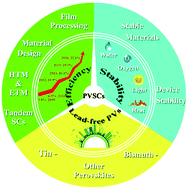
Shida Yang, Weifei Fu, Zhongqiang Zhang, Hongzheng Chen, Chang-Zhi Li
In this review, we first highlighted recent progress in high-performance perovskite solar cells (PVSCs) with a discussion of the fabrication methods and PVSCs-based tandem solar cells. Furthermore, the stability issue of PVSCs and strategies to improve material and device stability have been discussed, and finally, a summary of the recent progress in lead-free perovskites has been presented.
The content of this RSS Feed (c) The Royal Society of Chemistry