limno_lit
Shared posts
[ASAP] Extending the Family of Hybrid Layered Fluoride Perovskites
Excitons in Metal‐Halide Perovskites

This work aims to report a critical overview of recent progress in exciton physics of metal‐halide perovskites. These semiconductors are the subject of very intense study thanks to the unprecedented success in energy harvesting and light emitting applications. Interestingly the development of perovskite based devices has significantly outpaced understanding of their fundamental properties. One of the biggest puzzles of perovskites is related to exciton binding energy and its fine structure which are crucial for optoelectronic applications.
Abstract
The unprecedented increase of the power conversion efficiency of metal‐halide perovskite solar cells has significantly outpaced the understanding of their fundamental properties. One of the biggest puzzles of perovskites has been the exciton binding energy, which has proved to be difficult to determine experimentally. Many contradictory reports can be found in the literature with values of the exciton binding energy from a few meV to a few tens of meV. In this review the results of the last few years of intense investigation of the exciton physic in perovskite materials are summarized. In particular a critical overview of the different experimental approaches used to determine exciton binding energy is provided. The problem of exciton binding energy in the context of the polar nature of perovskite crystals and related polaron effects which have been neglected to date in most of work is discussed. It is shown that polaron effects can reconcile at least some of the experimental observations and controversy present in the literature. Finally, the current status of the exciton fine structure in perovskite materials is summarized. The peculiar carrier–phonon coupling can help to understand the intriguing efficiency of light emission from metal‐halide perovskites.
What Are the Ground State Structures of C20 and C24? An Explicitly Correlated Ab Initio Approach
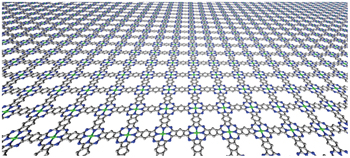
Rationally synthesized two-dimensional polymers

Nature Chemistry. doi:10.1038/nchem.1628
Authors: John W. Colson & William R. Dichtel
Two-dimensional polymers, which exhibit periodic bonding in two orthogonal directions, offer mechanical, electronic and structural properties distinct from their linear or irregularly crosslinked polymer counterparts. Their potential is largely unexplored because versatile and controlled synthetic strategies are only now emerging. This Review describes recent developments in two-dimensional polymerization methods.
Microstructure formation in molecular and polymer semiconductors assisted by nucleation agents
Nature Materials. doi:10.1038/nmat3655
Authors: Neil D. Treat, Jennifer A. Nekuda Malik, Obadiah Reid, Liyang Yu, Christopher G. Shuttle, Garry Rumbles, Craig J. Hawker, Michael L. Chabinyc, Paul Smith & Natalie Stingelin
Additives, including nucleating agents, have been used to regulate the solidification process of (semi-)crystalline polymer solids and thus control both their crystallite dimensions and shape. Here, we demonstrate that minute amounts (0.1–1 wt%) of commercially available nucleating agents can be used to efficiently manipulate the solidification kinetics of a wide range of organic semiconductors—including poly(3-alkylthiophene)s, the fullerene derivative [6,6]-phenyl-C61-butyric acid methyl ester (PCBM) and 6,13-bis(triisopropyl-silylethynyl) (TIPS) pentacene—when processed from the melt, solution or solid state, without adversely affecting the semiconductors’ electronic properties. Heterogeneous nucleation increases the temperature of and rate of crystallization of poly(3-alkylthiophene)s, permits patterning of crystallites at pre-defined locations in PCBM, and minimizes dewetting of films of TIPS-pentacene formed by inkjet printing. Nucleating agents thus make possible the fabrication of thin-film transistors with uniform electrical characteristics at high yield.
Organic semiconductors: Made to order
Nature Materials. doi:10.1038/nmat3686
Author: Antonio Facchetti
Fabricating thin films of organic semiconductors that have molecular order across large areas has proved challenging. Now, three complementary approaches — molecular design, fluid-flow control and the use of nucleating agents — offer unprecedented opportunities for next-generation optoelectronic applications.
Solution coating of large-area organic semiconductor thin films with aligned single-crystalline domains
Nature Materials. doi:10.1038/nmat3650
Authors: Ying Diao, Benjamin C-K. Tee, Gaurav Giri, Jie Xu, Do Hwan Kim, Hector A. Becerril, Randall M. Stoltenberg, Tae Hoon Lee, Gi Xue, Stefan C. B. Mannsfeld & Zhenan Bao

