13 Jun 11:43
Nanoscale, 2014, Advance Article
DOI: 10.1039/C4NR02025A, Review Article
Bryan D. Anderson, Joseph B. Tracy
Review article discussing recent advances in conversion chemistry of nanoparticles through the Kirkendall effect, galvanic exchange, and anion exchange.
To cite this article before page numbers are assigned, use the DOI form of citation above.
The content of this RSS Feed (c) The Royal Society of Chemistry

05 Jun 08:51
by Wanlin Guo
Nature Nanotechnology 9, 413 (2014).
doi:10.1038/nnano.2014.106
Authors: Wanlin Guo & Xiaofei Liu
Subnanometre metallic wires can be engineered from semiconducting sheets of transition-metal dichalcogenides by means of a focused electron beam.

27 May 08:34
by Yamamoto, Y., Arai, S., Esaki, A., Ohyama, J., Satsuma, A., Tanaka, N.
We have developed a quantitative particle size analytical method at the single atomic level employing electron microscopy and image processing for the investigation of supported metal catalysts. In the present study, a supported gold (Au) catalyst containing sub-nano clusters and individual atoms was globally observed by high-resolution high-angle annular dark-field scanning transmission electron microscopy (HAADF-STEM) using spherical aberration (Cs)-corrected TEM. To fully extract structural information of the Au clusters and individual atoms from the HAADF-STEM images, a morphological image-processing operation was applied. The resulting mean particle size was in good agreement with particle sizes estimated from average information provided by X-ray absorption fine structure analysis. It is demonstrated that the present HAADF-STEM image analysis gives a quantitative particle size distribution measurement of supported Au clusters and individual atoms.
12 May 10:51
by Eduardo M. Perassi, Calin Hrelescu, Andreas Wisnet, Markus Döblinger, Christina Scheu, Frank Jäckel, Eduardo A. Coronado and Jochen Feldmann

ACS Nano
DOI: 10.1021/nn406270z

12 May 10:35
Publication date: November 2014
Source:Ultramicroscopy, Volume 146
Author(s): Suhyun Kim , Younheum Jung , Sungho Lee , Joong Jung Kim , Gwangseon Byun , Sunyoung Lee , Haebum Lee
Spherical aberration correction in high-angle annular dark-field scanning transmission electron microscopy (HAADF-STEM) allows us to form an electron probe with reduced depth of field. Using through-focal HAADF imaging, we experimentally demonstrated 3D strain measurement in a strained-channel transistor. The strain field distribution in the channel region was obtained by scanning an electron beam over a plan-view specimen. Furthermore, the decrease in the strain fields toward the silicon substrate was revealed at different focal planes with a 5-nm focal step. These results demonstrate that it is possible to reconstruct the 3D strain field in electronic devices.
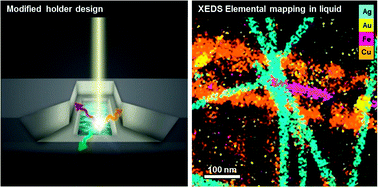
09 May 13:01
Chem. Commun., 2014, 50,10019-10022
DOI: 10.1039/C4CC02743D, Communication
Edward A. Lewis, Sarah J. Haigh, Thomas J. A. Slater, Zheyang He, Matthew A. Kulzick, M. Grace Burke, Nestor J. Zaluzec
A new design of in situ liquid cells is demonstrated, providing the first nanometer resolution elemental mapping of nanostructures in solution.
The content of this RSS Feed (c) The Royal Society of Chemistry

09 May 13:01
by Bart Goris, Lakshminarayana Polavarapu, Sara Bals, Gustaaf Van Tendeloo and Luis M. Liz-Marzán

Nano Letters
DOI: 10.1021/nl500593j

06 May 12:56
Publication date: November 2014
Source:Micron, Volume 66
Author(s): K.J. O'Shea , D. McGrouther , C.A. Ferguson , M. Jungbauer , S. Hühn , V. Moshnyaga , D.A. MacLaren
We describe a technique using a focused ion beam instrument to fabricate high quality plan-view specimens for transmission electron microscopy studies. The technique is simple, site-specific and is capable of fabricating multiple large, >100μm2 electron transparent windows within epitaxially grown thin films. A film of La0.67Sr0.33MnO3 is used to demonstrate the technique and its structural and functional properties are surveyed by high resolution imaging, electron spectroscopy, atomic force microscopy and Lorentz electron microscopy. The window is demonstrated to have good thickness uniformity and a low defect density that does not impair the film's Curie temperature. The technique will enable the study of in-plane structural and functional properties of a variety of epitaxial thin film systems.
06 May 12:53
by William J. Baumgardner, Yingchao Yu, Robert Hovden, Shreyas Honrao, Richard G. Hennig, Héctor D. Abruña, David Muller and Tobias Hanrath

ACS Nano
DOI: 10.1021/nn501543d

04 May 15:45
by Chunxing She, Igor Fedin, Dmitriy S. Dolzhnikov, Arnaud Demortière, Richard D. Schaller, Matthew Pelton and Dmitri V. Talapin

Nano Letters
DOI: 10.1021/nl500775p

30 Apr 16:06
Nanoscale, 2014, Advance Article
DOI: 10.1039/C4NR00708E, Review Article
D. Jaque, L. Martinez Maestro, B. del Rosal, P. Haro-Gonzalez, A. Benayas, J. L. Plaza, E. Martin Rodriguez, J. Garcia Sole
The state of the art regarding the use of nanoparticles for photothermal therapies is reviewed in detail.
To cite this article before page numbers are assigned, use the DOI form of citation above.
The content of this RSS Feed (c) The Royal Society of Chemistry

30 Apr 08:36
Publication date: October 2014
Source:Ultramicroscopy, Volume 145
Author(s): Takeo Sasaki , Hidetaka Sawada , Fumio Hosokawa , Yuta Sato , Kazu Suenaga
The performance of aberration-corrected (scanning) transmission electron microscopy (S/TEM) at an accelerating voltage of 15kV was evaluated in a low-voltage microscope equipped with a cold-field emission gun and a higher-order aberration corrector. Aberrations up to the fifth order were corrected by the aberration measurement and auto-correction system using the diffractogram tableau method in TEM and Ronchigram analysis in STEM. TEM observation of nanometer-sized particles demonstrated that aberrations up to an angle of 50mrad were compensated. A TEM image of Si[110] exhibited lattice fringes with a spacing of 0.192nm, and the power spectrum of the image showed spots corresponding to distances of 0.111nm. An annular dark-field STEM image of Si[110] showed lattice fringes of (111) and (22¯0) planes corresponding to lattice distances of 0.314nm and 0.192nm, respectively. At an accelerating voltage of 15kV, the developed low-voltage microscope achieved atomic-resolution imaging with a small chromatic aberration and a large uniform phase.
25 Apr 12:33
Nanoscale, 2014, 6,7204-7208
DOI: 10.1039/C4NR00935E, Communication
Jian Wang, Huile Jin, Yuhua He, Dajie Lin, Aili Liu, Shun Wang, Jichang Wang
This research presents a template-free solvothermal method which offers selective preparation of graphene ranging from two-dimensional sheets to 3-dimensional nanospheres.
The content of this RSS Feed (c) The Royal Society of Chemistry

23 Apr 09:53
by Nikos Liakakos, Christophe Gatel, Thomas Blon, Thomas Altantzis, Sergio Lentijo-Mozo, Cécile Garcia-Marcelot, Lise-Marie Lacroix, Marc Respaud, Sara Bals, Gustaaf Van Tendeloo and Katerina Soulantica

Nano Letters
DOI: 10.1021/nl500734k

22 Apr 17:44
Publication date: September 2014
Source:Ultramicroscopy, Volume 144
Author(s): Y.Q. Chen , T.J.A. Slater , E.A. Lewis , E.M. Francis , M.G. Burke , M. Preuss , S.J. Haigh
Energy-dispersive X-ray (EDX) spectroscopy in the scanning transmission electron microscope (STEM) has been used to demonstrate the presence of size-dependent compositional variation for L12-structured Ni3Al-type gamma-prime (γ′) precipitates within a commercial RR1000 Ni-based superalloy. This semi-quantitative elemental analysis has been achieved using electrochemical extraction of the γ′ precipitates from the γ matrix. The applicability of this approach to size-dependent compositional analysis of precipitates was confirmed by a comparison of the size distribution for the extracted precipitates with those present in traditional electropolished foil specimens in the size range 20–250nm. By applying suitable thickness-dependent absorption-corrections we have demonstrated that the composition of γ′ precipitates in our material depends on the size of the precipitate in the range of 5nm to 3μm. In particular, the Al content was observed to increase in smaller γ′ precipitates while Ti and Ta contents are constant for all sizes of precipitate. Hf was observed to be present only in the largest precipitates. This type of local compositional information provides invaluable input to assess the accuracy of microstructural modelling for these complex alloys and provides new evidence supporting the importance of anti-site diffusion.
22 Apr 15:10
Nanoscale, 2014, 6,6569-6576
DOI: 10.1039/C4NR01918K, Paper
Ossi Lehtinen, I.-Ling Tsai, Rashid Jalil, Rahul R. Nair, Juhani Keinonen, Ute Kaiser, Irina V. Grigorieva
A novel method for non-invasive imaging of vacancy defects in graphene by high-resolution transmission electron microscopy is demonstrated and used to show that ion irradiation of graphene produces reconstructed monovacancies.
The content of this RSS Feed (c) The Royal Society of Chemistry

22 Apr 09:20
by Ruibin Jiang, Benxia Li, Caihong Fang, Jianfang Wang
Hybrid nanostructures composed of semiconductor and plasmonic metal components are receiving extensive attention. They display extraordinary optical characteristics that are derived from the simultaneous existence and close conjunction of localized surface plasmon resonance and semiconduction, as well as the synergistic interactions between the two components. They have been widely studied for photocatalysis, plasmon-enhanced spectroscopy, biotechnology, and solar cells. In this review, the developments in the field of (plasmonic metal)/semiconductor hybrid nanostructures are comprehensively described. The preparation of the hybrid nanostructures is first presented according to the semiconductor type, as well as the nanostructure morphology. The plasmonic properties and the enabled applications of the hybrid nanostructures are then elucidated. Lastly, possible future research in this burgeoning field is discussed.

(Plasmonic metal)/semiconductor hybrid nanostructures are currently of increasing interest owing to their rich and attractive physical and chemical properties derived from localized plasmon resonance and semiconduction. In this article, the preparation, properties, and applications of this type of hybrid nanostructure are reviewed. Future directions in this field are also discussed.
16 Apr 09:02
by Jianming Zheng, Meng Gu, Arda Genc, Jie Xiao, Pinghong Xu, Xilin Chen, Zihua Zhu, Wenbo Zhao, Lee Pullan, Chongmin Wang and Ji-Guang Zhang

Nano Letters
DOI: 10.1021/nl500486y

04 Apr 16:42
Nanoscale, 2014, 6,6646-6650
DOI: 10.1039/C4NR01100G, Paper
Lluis Yedra, Alberto Eljarrat, Jose Manuel Rebled, Lluis Lopez-Conesa, Nico Dix, Florencio Sanchez, Sonia Estrade, Francesca Peiro
Novel TEM 4D characterization: electron tomogram containing a core-loss spectrum per voxel.
The content of this RSS Feed (c) The Royal Society of Chemistry

01 Apr 13:21
Nanoscale, 2014, 6,6245-6266
DOI: 10.1039/C4NR00612G, Review Article
Kim Truc Nguyen, Yanli Zhao
This review highlights recent significant advances of graphene/nanoparticle hybrids for electronics and biological applications.
The content of this RSS Feed (c) The Royal Society of Chemistry

25 Mar 14:36
by Jingyu Lu, Zainul Aabdin, N. Duane Loh, Dipanjan Bhattacharya and Utkur Mirsaidov

Nano Letters
DOI: 10.1021/nl500766j

25 Mar 14:36
by Ryo Ishikawa, Andrew R. Lupini, Scott D. Findlay, Takashi Taniguchi and Stephen J. Pennycook

Nano Letters
DOI: 10.1021/nl500564b

20 Mar 08:19
Publication date: October 2014
Source:Ultramicroscopy, Volume 145
Author(s): C.B. Boothroyd , M.S. Moreno , M. Duchamp , A. Kovács , N. Monge , G.M. Morales , C.A. Barbero , R.E. Dunin-Borkowski
We present an atomic resolution transmission electron microscopy (TEM) and scanning TEM (STEM) study of the local structure and composition of graphene oxide modified with Ba2+. In our experiments, which are carried out at 80kV, the acquisition of contamination-free high-resolution STEM images is only possible while heating the sample above 400°C using a highly stable heating holder. Ba atoms are identified spectroscopically in electron energy-loss spectrum images taken at 800°C and are associated with bright contrast in high-angle annular dark-field STEM images. The spectrum images also show that Ca and O occur together and that Ba is not associated with a significant concentration of O. The electron dose used for spectrum imaging results in beam damage to the specimen, even at elevated temperature. It is also possible to identify Ba atoms in high-resolution TEM images acquired using shorter exposure times at room temperature, thereby allowing the structure of graphene oxide to be studied using complementary TEM and STEM techniques over a wide range of temperatures.
13 Mar 12:24
by Se-Woong Baek, Garam Park, Jonghyeon Noh, Changsoon Cho, Chun-Ho Lee, Min-Kyo Seo, Hyunjoon Song and Jung-Yong Lee

ACS Nano
DOI: 10.1021/nn500222q

13 Mar 12:21
by Qingmei Su, Gaohui Du, Jun Zhang, Yijun Zhong, Bingshe Xu, Yuehai Yang, Suman Neupane and Wenzhi Li

ACS Nano
DOI: 10.1021/nn500194q

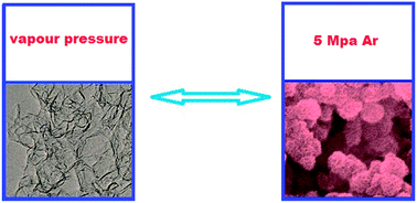
10 Mar 14:14
by Darius Pohl, Ulrich Wiesenhütter, Elias Mohn, Ludwig Schultz and Bernd Rellinghaus

Nano Letters
DOI: 10.1021/nl404268f

06 Mar 16:40
Publication date: January 2014
Source:Ultramicroscopy, Volume 136
Author(s): A. Grenier , S. Duguay , J.P. Barnes , R. Serra , G. Haberfehlner , D. Cooper , F. Bertin , S. Barraud , G. Audoit , L. Arnoldi , E. Cadel , A. Chabli , F. Vurpillot
The structural and chemical properties of advanced nano-devices with a three-dimensional (3D) architecture have been studied at the nanometre scale. An original method has been used to characterize gate-all-around and tri-gate silicon nanowire transistor by combining electron tomography and atom probe tomography (APT). Results show that electron tomography is a well suited method to determine the morphological structure and the dimension variations of devices provided that the atomic number contrast is sufficient but without an absolute chemical identification. APT can map the 3D chemical distribution of the atoms in devices but suffers from strong distortions in the dimensions of the reconstructed volume. These may be corrected using a simple method based on atomic density correction and electron tomography data. Moreover, this combination is particularly useful in helping to understand the evaporation mechanisms and improve APT reconstructions. This paper demonstrated that a full 3D characterization of nano-devices requires the combination of both tomography techniques.
06 Mar 16:40
by Haihua Liu, Oh-Hoon Kwon, Jau Tang and Ahmed H. Zewail

Nano Letters
DOI: 10.1021/nl404354g

06 Mar 16:37
Publication date: May 2014
Source:Ultramicroscopy, Volume 140
Author(s): Robert Hovden , Peter Ercius , Yi Jiang , Deli Wang , Yingchao Yu , Héctor D. Abruña , Veit Elser , David A. Muller
To date, high-resolution (<1nm) imaging of extended objects in three-dimensions (3D) has not been possible. A restriction known as the Crowther criterion forces a tradeoff between object size and resolution for 3D reconstructions by tomography. Further, the sub-Angstrom resolution of aberration-corrected electron microscopes is accompanied by a greatly diminished depth of field, causing regions of larger specimens (>6nm) to appear blurred or missing. Here we demonstrate a three-dimensional imaging method that overcomes both these limits by combining through-focal depth sectioning and traditional tilt-series tomography to reconstruct extended objects, with high-resolution, in all three dimensions. The large convergence angle in aberration corrected instruments now becomes a benefit and not a hindrance to higher quality reconstructions. A through-focal reconstruction over a 390nm 3D carbon support containing over 100 dealloyed and nanoporous PtCu catalyst particles revealed with sub-nanometer detail the extensive and connected interior pore structure that is created by the dealloying instability.
06 Mar 16:28
by Alex W. Robertson, Gun-Do Lee, Kuang He, Euijoon Yoon, Angus I. Kirkland and Jamie H. Warner

Nano Letters
DOI: 10.1021/nl500119p

No more posts. Check out what's trending.