Shared posts

05 Jul 16:51

Квазиоптика в диапазоне 3мм

Stepan

Да, миллиметры - это жопа :(

Добрый день!

Периодически нуждаюсь в консультациях по данной тематике. Микроволны в образовании были, но, как говорится - выучил частично, но сдал полностью. В основном работал с НЧ аналоговой техникой, к микроволнам пришел сравнительно недавно, лет 20 назад )). Микроволновая часть была проработана остепененным специалистом, которого теперь нет. От него получал готовые к установке комплекты.

Занят разработкой и изготовлением приборов измерения поглощения микроволн некоторыми материалами. Сейчас пользую диапазон 3мм. Схема измерения из учебника - излучение "просвечивает" материал, два приемных детектора контролируют мощности входа и выхода, далее логарифм отношения. Детекторные и генераторный модули непосредственно соединяются с рупорными облучателями, далее сплошная оптика - линза из фторопласта корректирует фазу фронта, диск развязки с поглощающим материалом и согласующими пленками, ответвитель из пленки на 45 градусов...

С утратой специалиста многое пришлось осваивать - материал поглотителя, согласующая пленка, геометрия линз. Но вопросы все появляются. Например сейчас ищутся допуски геометрии стандартного фланца волновода 2,4х1,2мм (стык модулей с рупорами).

Отзовитесь кто имел дело с подобными вещами.

05 Jul 16:50

Импорт GERBER в ЭМ симулятор

Stepan

Хоть бы кто почитал СВЧушки...

Здравствуйте. Возникла необходимость просимулировать работу высокоскоростной линии. В наличии имеется только gerber. Может кто знает в какой пакет можно импортировать gerber файл двухсторонней платы? Пробовал в hyperlynx но так и не получилось нормально импортировать.

24 Jun 13:10

подходы к согласованию на два возможных импеданса антенны?

Stepan

Интересная тема. К слову о тюнерах импеданса.

Простите за пробелы в образовании. Какие существуют подходы к согласованию антенны на изменяющийся импеданс? Грубо говоря на два значения, на нормальную ее работу, и когда ее схватили рукой? Под один приемник.

04 May 15:19

Вопрос по намотке катушки для ВЧ фильтра

Stepan

Да, жизненно :)

Здравствуйте. Есть потребность в изготовлении полоснопропускающего фильтра. Частота порядка 400 МГц. Индуктивность одной из катушек по расчёту получилась 1.4 нГн. Как такую катушку можно сделать? Чтобы еще и добротная была. В coil32 пробовал посчитать, получается, что там даже нет и одного витка при такой индуктивности.

15 Apr 15:00

Let’s Learn Together: Electromagnetics Engineer Role

by Katie Corey
Stepan

Ништяк! Это прям про меня :)

This post is a continuation in a series about simulation on the 3DEXPERIENCE platform and some of the roles you can find there. This week we are focusing on the Electromagnetics Engineer Role and how it enables designers and engineers to perform electromagnetic simulations from low to high frequency (static to optical), including the optimization of antennas, microwave components, and electro-mechanical devices.


Overview

The SIMULIA Electromagnetics Engineer role delivers electromagnetic simulation powered by industry-proven CST Studio Suite technology in a seamless, intuitive, and modern user interface connected with the 3DEXPERIENCE®  platform.

It enables designers and engineers to perform electromagnetic simulations from low to high frequency (static to optical), including the optimization of antennas, microwave components, and electro-mechanical devices. SIMULIA Electromagnetics Engineer enables design teams to improve product performance, reduce time-to-market and minimize device malfunctions, warranty claims, and recalls.

SIMULIA Electromagnetics Engineer offers a broad range of solution methods with a unique capability to identify and mitigate electromagnetic compatibility (EMC) and electromagnetic interference (EMI) risks in electronic devices. Additionally, the technology can be applied to simulation of human body exposure to electromagnetic fields. Electromagnetic Engineer ensures that the device passes any certification tests required by regulatory and industry standards the first time.

Key Functionalities

The SIMULIA Electromagnetics Engineer role delivers proven best-in-class CST Studio Suite technology used in leading technology and engineering companies around the world. It offers:

  • Powerful simulation methods such as the unique finite integration technique (FIT), the classical finite element method (FEM), the transmission line matrix method (TLM), and also hybrid simulation methods
  • Specialized solvers for applications such as motors, printed circuit boards, cable harnesses, and filters
  • Coupled simulations: system-level, multiphysics, field/circuit co-simulation to deliver unprecedented simulation reliability and accuracy
  • An All-in-one fully parametric design environment for modeling
  • A wide range of complex material models
  • Powerful post-processing and visualization tools
  • Built-in optimizers
  • High-performance computing on workstations and on clusters: multi-threading, GPU and hardware acceleration, distributed computing and MPI multi-process parallelization (like MPI)
  • Cloud computing* on the 3DEXPERIENCE platform to submit and monitor CST Studio Suite jobs from anywhere

Benefits

The SIMULIA Electromagnetics Engineer role:

  • Provides access to SIMULIA CST Studio Suite, the leading solution for low to high frequency (static to optical) electromagnetic simulations
  • Supports engineers for antenna and microwave devices design to improve product performance and reduce time-to-market
  • Helps engineers to identify and mitigate electromagnetic compatibility (EMC) and electromagnetic interference (EMI) risks in electronic devices, minimizing warranty claims and recalls
  • Consumes parametric SOLIDWORKS and CATIA design data from the 3DEXPERIENCE platform to perform electromagnetic simulation

Highlights

  • Powerful simulation methods such as the unique finite integration technique (FIT), the classical finite element method (FEM), the transmission line matrix method (TLM), and also hybrid simulation methods
  • Specialized solvers for applications such as motors, printed circuit boards, cable harnesses, and filters
  • Coupled simulations: system-level, multiphysics, field/circuit co-simulation to deliver unprecedented simulation reliability and accuracy
  • A wide range of complex material models
  • Powerful post-processing and visualization tools
  • Built-in optimizers


SIMULIA offers an advanced simulation product portfolio, including AbaqusIsightfe-safeToscaSimpoe-MoldSIMPACKCST Studio SuiteXFlowPowerFLOW, and more. The SIMULIA Community is the place to find the latest resources for SIMULIA software and to collaborate with other users. The key that unlocks the door of innovative thinking and knowledge building, the SIMULIA Community provides you with the tools you need to expand your knowledge, whenever and wherever.

15 Apr 14:48

Dalmaris Peter. Kicad Like a Pro [DJVU] (43,59 МБ)

Stepan

Это сильно...

3rd Edition. Tech Explorations, 2022. 1081 p. ISBN: 978-1-68489-093-4. If you have never used KiCad and have little or no experience in PCB design, you should read this book it in a linear fashion. The first few chapters will give you the fundamental knowledge on which you will build your skill with the projects later in the book. If you have a good working knowledge of...
15 Apr 14:43

Умножитель частоты на 3

Stepan

Ключевое требование - на отечественных компонентах...

Добрый день! Кто-нибудь подскажет рабочую схему утроителя частоты на отечественных планарных компонентах? Необходимо умножить 800 МГц на 3 без ухудшения фазовых шумов относительно 20lgN. Уровень фазовых шумов 800 МГц: -150 дБн/Гц@10кГц, -160 дБн/Гц@100кГц.

15 Apr 14:42

Балун, двойной балансный смеситель, потери преобразования

Stepan

Мистика...

Добрый вечер!

1.Промоделировал симметрирующий трансформатор со средней точкой (BALUN)

7.thumb.jpg.666c69987334c7e2c4c3d5b41061c796.jpg

2. АЧХ и ФЧХ балуна

5.thumb.jpg.603fe13e0918d962ee261423d3a73988.jpg

6.thumb.jpg.d8723a555baa8d23fbefca8657dc0024.jpg

3. Схема двойного балансного смесителя на основе балунов и диодов шоттки (Up-converter. IF==0.1 (5) ГГц, LO - свипируется в диапазоне от 1 до 40 ГГц)

8.thumb.jpg.5e5e324bc29094482c8d9739ce4e21ef.jpg

4. Дичайшие!!! потери преобразования (при малом 0.1 ГГц IF)

9.thumb.jpg.44fe355767ed3e851b15f8bc3691b8da.jpg

5. Изменяю частоту IF с 0.1 ГГц на 5 ГГЦ, потери преобразования уменьшились, но всё равно дикие!!!

15.thumb.jpg.cce198dd372c4e7a5bff9e9afa912f3a.jpg

6. Заменяю промоделированный трансформатор на идеальный. Потери (при +15 дБм и +21 дБм гетеродина) преобразования лучше чем у Marki Microwave :good:

13.thumb.jpg.06d3b60f26b5f37398dda8ec10669d2e.jpg

14.thumb.jpg.d269d9f191a2ebeb7bee44a935890d7e.jpg

Странное поведение, ведь в диапазоне от 12 до 20 ГГц коэффициент передачи трансформатора -3.8дБ (дисбаланс фазы 2 сотых и 8 десятых градуса на краях). 

Откуда такие потери??? :help:

Используя гораздо более узкополосный балун (но без средней точки) потери преобразования получаются существенно лучше

16.thumb.jpg.94416daab87e0fecb2851db452e422c0.jpg

15 Apr 14:41

ФИЛЬТР на выходе ПРД

Stepan

Ну и что, подсказали?

Добрый день!

Необходим "железный" фильтр на выходе передатчика. Параметру ПРД: частота несущей 1900 МГц, полоса 12 МГц, выходная мощность 6 Вт.

Выбор стоит между фильтром на встречных стержнях и на коакиальных резонаторах, типа таких:

image.png.23a445bd4ddb7f04c452579c521a3625.png

image.png.a0eed2e9e636b35ff55ca58c557a1150.png  


 Можете подсказать достоинства и недостатки этих фильтров. Нужен сравнительный анализ 


30 Mar 14:10

Импортозамещение импортом?

Stepan

Печаль :(

Уважаемые коллеги! В связи с непростой обстановкой с ввозом импорта в Россию решил создать данную тему.

Предлагаю делиться контактами производителей СВЧ электроники в России (не зависящие от санкционных foundry), или в странах не вводивших для России санкции.

Возможно кто-то захочет прорекламировать своё производство.

Может у кого-то есть опыт работы с китайской СВЧ ЭКБ?

Меня интересует как маломощные компоненты (МШУ, фазовращатели, смесители и т.д.) так и мощные СВЧ транзисторы в L и S диапазоне.

Предлагаю в этой теме в принципе делиться любым опытом, который может нам помочь в сложившийся ситуации.

30 Mar 14:08

Антенная решетка с диэлектрической линзой

Stepan

Интересная тема.

Доброго времени суток. Есть задача по увеличению коэффициента усиления антенны за счет использования диэлектрической линзы. Есть отдельная антенная решетка, состоящая из 4 патчей, и диэлектрическая линза. При совмещении их и запуске моделирования получается, что коэффициент усиления и диаграмма направленности остаются такие же, как и без линзы. Возможно кто поможет по объединению в один проект и получения адекватных результатов при использовании диэлектрической линзы.

С уважением, Максим

Безымянный.png

15 Dec 10:49

Разъёмы для большого уровня мощности в диапазоне до 4 ГГц

Stepan

Интересный вопрос...

Здравствуйте, коллеги.

Я задался вопросом выбора разъёмов для работы на мощности 1,5 кВт в диапазоне частот до 4 ГГц. Я, к сожалению, не могу сообщить, где это будет применяться, но это, как мне кажется в этом обсуждении будет не важно: просто предположим, что такое устройство есть (или должно быть).

Итак, у меня есть каталог фирмы Huber&Suhner, несколько даташитов фирм Rosenberger и Ampheon, всё для разъёмов типа N и 7/16 -- и вот тут начинается моё непонимание. Есть два вида параметров, указанных в этих документах, причём они никогда не встречаются вместе: это DWV (dielectric withstanding voltage) и Power Handling в виде графиков или чисел. Значения для этих параметров отличаются на 1-2 порядка (если пересчитать напряжение в мощность).

Первый параметр мне понятен -- это скорее всего напряжение диэлектрического пробоя для того диэлектрика, которым заполнен разъём и оно действительно может быть достаточно велико (указаны числа от 1000 до 3000 Vrms).

Но вот со вторым параметром, значения которого представляются мне более близкими к правде, у меня трудность и непонимание (сразу прошу простить за возможно наивные вопросы):

  • почему мощность падает с увеличением частоты?
  • почему, например, для разъёма типа N предельный уровень мощности на частоте 1000 МГц составляет около 750 Вт (при согласовании с линией до КСВН 1,0), хотя мой опыт показывает, что они используются на гораздо больших (импульсных мощностях)?
  • это ограничение по мощности связано с тепловыми потерями в разъёме?
  • на что ориентироваться при указании мощностных ограничений при использовании моего гипотетического устройства в диапазоне частот от 0 до 4 ГГц?

В качестве иллюстрации привожу график из каталога H&S:


Spoiler

Screenshot_2.thumb.png.09a60b05e382a533be7daf151b34a7db.png


Буду очень признателен за ответные реплики!

03 Dec 13:45

Согласование ВЧ транзистора

Stepan

Вот она - "ебля с плясками" :)

Добрый день. Прошу совета.

1)Сделал плату усиления на одном ВЧ транзисторе CGH55015F2 с согласующими дорожками под импеданс ,приведенный даташите под тестовую плату;

2)Завел транзистор, подал вч сигнал 0 дбм, получил на выходе -20 дБм, транзистор КУ регулирует на 10 дбм).

По какому пути идти, чтобы довести макет до ума. Как снять импеданс входа выхода подручными средствами?

Есть ВЧ генератор, анализатор спектра и анаализатор векторных цепей.

Фото приложу. 

Есть вторая согласующая дорожка с квадратиками для изменения топологии согласующей цепи.

Подключить на входе и выходе регулировачную емкость и индуктивность паралельно поледнему/первому участку согласующих цепей?

IMG_20211201_104354.jpg

18 Nov 15:21

Поиск модели антенны, или аналога

Stepan

Ну так себе...

RF Antenna - Wieson Technologies
Подборка wifi антенн.
Задачка:
1. Смоделировать в корпусе ноута со всеми деталями в сборе.
2. Может быть у кого-то есть готовые модельки хотя бы аналогичных антенн? Поделитесь пожалуйста. Благодарю.

12 Nov 15:08

EMC Fundamentals: Pre-compliance Testing Using a Real-time Oscilloscope

Stepan

Интересный материал. Жаль, что я его очень плохо понял.

Poorly designed interconnects can contribute to near field emissions, which is sometimes an indication of EMI failures, read on to see how to avoid failing an FCC test.

12 Nov 15:03

Antenna and Sensor Design for ADAS and AV

by Clare Scott
Stepan

Как-то мало интересных картинок.

This blog was originally published as a whitepaper, which you can download here


Advanced driver assistance systems (ADAS) offer an extra layer of safety and convenience while driving. Besides that, they are also an important step towards fully autonomous vehicles. Radar, vehicle-to-vehicle communication, 5G connectivity, smart road infrastructure and satellite navigation all help ADAS systems be aware of their surroundings, and all these systems heavily rely on antennas and sensors to function.

Placing antennas on vehicles poses several challenges. The body of a car can strongly influence the antenna performance, reducing efficiency and changing the field pattern. Different systems can interfere with each other and other sensitive on-board electronics. Water and dirt can also soil antennas and sensors, reducing their effectiveness. Simulation supports antenna and sensor system design and integration by allowing engineers to analyze their performance in real-world scenarios before committing to building a physical prototype.

EXECUTIVE SUMMARY

In order to safely control a vehicle, ADAS systems require full awareness of their surroundings—lane markings, signs, road conditions, other vehicles and road users, as well as unexpected obstacles. Vehicles equipped accordingly detect their environment through a number of techniques such as cameras, ranging systems like radar and lidar, geolocation, and other sensors located around the vehicle. Robust 5G and other high speed mobile data connectivity is also
critical to ensuring ADAS systems can interface with internet services, smart road infrastructure, other vehicles as well as the passengers’ own devices. The components that comprise these systems are sensitive to placement effects, dirt and snow soiling and interference from other antennas and electronics. These factors need to be addressed at the whole system level in order to design safe, reliable ADAS and autonomous drive systems.

CHALLENGES OF ADAS AND AUTONOMOUS DRIVING

Antennas and sensors are necessarily very sensitive to their surroundings. In order to allow them to operate safely and reliably, unwanted influences need to be minimized. This is particularly difficult when designing a vehicle with limited space for mounting components, which also has to drive in unpredictable and highly variable conditions. The metal body of the vehicle can block and reflect electromagnetic waves. The performance of an antenna on a curved car body can also be very different to the idealized datasheet characteristics, which generally assume a flat ground plane. This can lead to blind spots in coverage for safety
critical systems such as radar or cause spurious readings by affecting beam direction and side lobes. Therefore, component placement is critical to building an effective ADAS system.

Electromagnetic interference (EMI) from other components can also cause issues. Radio and radar antennas, power electronics and high-voltage systems (such as electric drive systems) for example, can all radiate fields or generate currents that affect sensor performance. Electromagnetic compatibility (EMC) is likewise an issue—the sensors must not interfere with other systems in the vicinity and surrounding vehicles. Similarly, the fields radiated by antennas and sensors must remain within radiation hazard (RADHAZ) exposure limits. Occupants as well as passersby need to be safe when radar sensors are operating. The specific absorption rate (SAR) for human tissue needs to be analyzed for different use cases and under varying load cases to ensure compliance with regulation. Finally, factors outside the vehicle can affect antenna performance. Other vehicles, the road environment, and the weather can all reflect or absorb electromagnetic waves. Labs and test tracks offer an opportunity to measure how ADAS systems perform in different environments, but testing all the different scenarios that can occur would be prohibitively expensive and time consuming.

BENEFITS OF SIMULATION

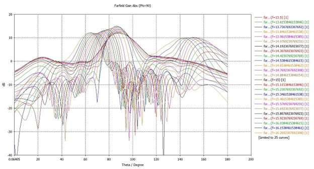
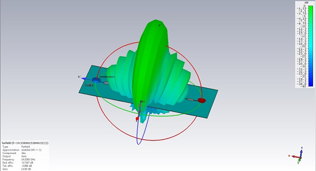
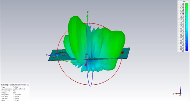
Introducing simulation in the ADAS design cycle can significantly reduce development times, costs and above all, risks, by addressing the challenges listed above. Electromagnetic simulation calculates the electric and magnetic fields and antenna farfield pattern, as well as other relevant key performance indicators (KPIs) such as directivity and gain. These can be determined through simulation long before building a physical prototype. A wider variety of configurations—such as different antenna types and placements—can be analyzed in parallel in order to optimize performance. For these analyses, CAD models are directly transferred into the simulation environment, allowing engineers to rapidly see how design changes affect ADAS performance.

Multiple antennas and sensors can be simulated together in situ on the same vehicle platform. This means that parasitic effects and interference are taken into account during the simulation. Other components that might cause interference, such as on-board electronics and electric drive systems, can also be included.
Furthermore, fluid simulation can be used to calculate the effect of rain and mud spray on sensors. The spray patterns, calculated at different speeds and in different conditions, help to identify potential issues before commencing wide scale test drives. Using the same model data for the electromagnetic and fluid simulation speeds up the process even further.

Vehicles can quickly travel tens or hundreds of virtual miles in simulation, covering a much wider variety of road scenarios than test driving alone could ever hope to match.

Collaboration and a combination of workflows to ensure vehicle safety and reliable connectivity

The increased complexity of ADAS and Autonomous Vehicles requires close collaboration between designers and engineering teams to solve the challenges and benefit from faster development cycles and reduced risk. Combining simulation workflows, and integrating simulation with other products, including CAD
and PLM, can help to meet the common requirements and engineering challenges of ADAS designers. Components developed by different groups can be quickly assembled into a full vehicle model and prepared for simulation, thus ensuring that simulation engineers are working with the latest versions of the geometry and keeping up with changes made to the underlying models.

Antenna design—quickly providing the right antenna for the given application

One of the first steps of developing any ADAS system is to find the correct component for the application. Antenna Magus offers a searchable catalogue of antenna designs, and will automatically select and suggest antennas that meet specifications such as size, technology, frequency and gain. These can then be used as a good starting point and give confidence for the final antenna optimization.

Comprehensive Technology for Electromagnetic Simulations: Access to all solvers via one user interface and single license

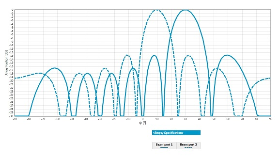
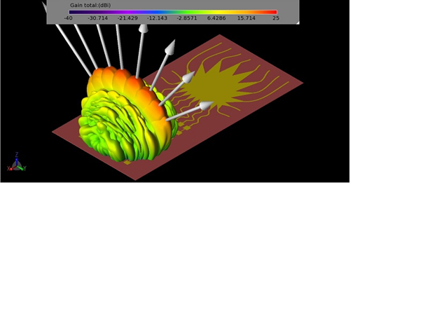
Antenna and sensor placement—calculate the KPIs for 5G, mobile data, radar, GPS and other antenna systems to find the optimal placement

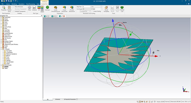
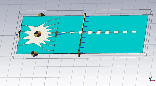
Once an appropriate antenna has been designed, it then has to be placed on the vehicle and integrated into the system at large. The electromagnetic simulation package CST Studio Suite allows engineers to calculate the KPIs of antennas and sensors when attached to the vehicle. Full wave 3D electromagnetic simulation can include the vehicle body, other electronics, and the surrounding environment, to ensure the component will behave as expected when mounted on the vehicle.

Avoid ghost target detection– complex geometry interacts with the radar system and can cause the detection of false positives, also known as ghost targets.

Co-site interference mitigation (RF desense)—identifying potential interference issues between systems

With so many components in close proximity, electromagnetic interference (EMI) and electromagnetic compatibility (EMC) are key concerns. The Interference Task in CST Studio Suite automatically identifies potential interference issues and produces an interference matrix showing which systems have the potential to interfere with each other. Engineers can quickly identify mitigation solutions, such as introducing additional filters or moving antennas to different locations to reduce interference to acceptable levels.

Human exposure compliance—ensuring that the exposure to electromagnetic fields remains within legal limits

Human exposure simulation: Radiated field within the driver cabin of a vehicle

Many classes of devices are subject to regulations on how much radio frequency (RF) power people near them may be safely exposed to. Realistic human body models can be added into the simulation environment and posed in and around the vehicle to allow exposure to be calculated without having to construct a costly prototype test set-up. KPIs, such as specific absorption rate (SAR), are automatically calculated by the simulation, allowing engineers to keep emitted radiation below regulatory limits.

Model-based-systems-engineering—defining and integrating system architecture up to full vehicle level

Before any components are nominated it is important to understand how the system as a whole is supposed to be designed. A methodology that has been used for decades in the aerospace industry, and is finding more and more favor in the automotive industry, is mode-lbased systems engineering. No Magic is the industry tool of choice to model systems and their interdependencies, and perform system level behavioral simulations. This is crucial in order to correctly size components and predict their performance.

Soiling optimization—modelling how rain, snow and mud spray can cover antennas and cameras

Fluid simulation, with PowerFLOW, models the behavior of rain, snow and mud spray and calculates whether their splatter can cover antennas and cameras. Using the results of the simulation, engineers can change the placement of sensors or adjust the design of the car body to reduce the risk of them being obscured.

Simulation of vehicle soiling during realistic driving scenarios.


Vehicle Drive-Scenario Simulation—Building virtual environments for virtual test driving

With higher levels of autonomy the number of miles driven has become the main metric by which the maturity of a system is measured. In order to prove the reliability of an autonomous system under countless driving and environmental scenarios it is vital to train the systems with a wide range of data. Driving millions or even billions of miles with prototype vehicles in real life is not feasible. Simulation in high fidelity virtual environments is key in order to reach those “miles driven” milestones. AVSimulation makes it easy to generate realistic virtual environments and then define a variety of driving scenarios to be analyzed therein. Tight coupling with the 3DEXPERIENCE platform ensures traceability and consistency across all steps of the engineering process.

SCANeR makes it possible to quickly build up high fidelity virtual environments to perform drive tests in. Simulation models are available at different levels of fidelity, from fully detailed physical models to lightweight models appropriate for real-time hardware in the loop evaluation.


Wire harness electrical engineering—optimizing the cabling between sensors and on board computers
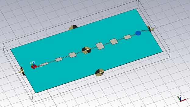
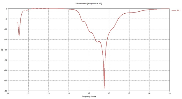
ADAS sensors and other components are connected by bus cables combined into complex wire harnesses. Interference between different cables and wires can degrade the performance of ADAS and the other on board systems. CST Studio Suite can import cable harness designs and simulate these complex interactions efficiently, quickly identifying possible crosstalk and signal integrity (SI) issues.

CONCLUSION

Creating safe and reliable ADAS and Autonomous Driving Systems requires close collaboration and integration of high fidelity multi-physics simulation. Designing components and systems without taking these complex interactions into account is not possible while ensuring peak performance and adequate time to market. A combined modeling and simulation approach gives designers and systems integrators the tools they need to build a “virtual twin” of both individual ADAS components and full systems as an integral part of the vehicle, for testing without the need for a physical prototype. Thus ‘vehicles’ can be driven millions or even billions of virtual miles in realistic high fidelity environments to validate ADAS systems in a huge variety of realistic scenarios.

Dassault Systèmes offers a complete end-to-end solution for ADAS design on the 3DEXPERIENCE® platform, powering collaboration and communication between different stakeholders, bringing together all the different components and other data into a single source of truth while also protecting confidential information, ensuring full traceability throughout the entire development process. Enterprises employing this approach can not only cut development time and cost, but unlock untapped innovation and reduce risk on their way to the next level of autonomous driving.


SIMULIA offers an advanced simulation product portfolio, including AbaqusIsightfe-safeToscaSimpoe-MoldSIMPACKCST Studio SuiteXFlowPowerFLOW and more. The SIMULIA Community is the place to find the latest resources for SIMULIA software and to collaborate with other users. The key that unlocks the door of innovative thinking and knowledge building, the SIMULIA Community provides you with the tools you need to expand your knowledge, whenever and wherever.


12 Nov 14:58

Как посчитать S-параметры и входной импеданс из полей в методе FDTD

Stepan

Ничего так человек погрузился в тему...

Здравствуйте!
Доселе не знал бед и использовал HFSS нажимая 2 кнопушки и получал готовый результат. Брал его на веру, отдавал начальству со словами я сделяль.

Сейчас появилась необходимость понять как работает вычислительная электродинамика... Решил начать с FDTD (не спрашивайте почему), изучил матчасть по электродинамике, вспомнил уравнения максвела, изучил тему распространения волны в изотропной среде, распространение в диэлектриках, освежил знания по линиям передач, волноводам, далее изучил основы метода FDTD в электродинамике, про "Yee Lattice",  методы решения и т.д. И вот вроде бы пора приступать от теории к действию: сделал пару простых упражнений с распространение волны в двумерном пространстве. Тоже вроде ок, поразбирался. Но мне как электронщику нужно знать не только характеристики E/H поля, но и такие вещи как V/I, S/Y/Z параметры (например для линии передач). И вот тут у меня затык...
В учебниках есть глава про уравнения распространения волны E/H и волны V/I (Transmission Line), но как из одного получить другое не совсем очевидно. Точнее очевидно, для получения поля V мы интегрируем поле E, для получения I интегрируем H по контуру. Но тут возникает один вопрос, а как этот контур выбрать и надо ли вообще это делать? Вручную? Как же тогда решатели в HFSS, EM в ADS определяют как им интегрировать и вычисляют эти характеристики? Помогите, пожалуйста, заполнить пробел. Что мне изучить, что порешать, где я что то упустил...

12 Nov 14:57

Расчет ГУН

Stepan

Я бы тоже не отказался.

Привет всем. 

Посоветуйте литературу по расчетам ГУН, желательно с примерами расчета. 

Зачем понадобилось - потребовалось переделать старый ГУН, собранный на bfg540+bb833, работал на частотах 1150...1400 МГц. На новом BFU550+ bb833 диапазон 900...1300 МГц при управляющих напряжениях до 9 вольт. ГУН запускается, но на частотах выше 1200 МГц крутизна падает с 60 до 10...15 и фапч с трудом захватывается. Пытаюсь понять как исправить. Заранее спасибо.

12 Nov 14:56

МЛА на основе Линзы Ротмана и решётки патчей

Stepan

Интересный проектик...

Уважаемые коллеги, специалисты по CST и антеннам!

Стояла задача рассчитать сканирующую антенну в широком секторе углов (минимум 90град) в Ku-band (14-16ГГц)

Вариант с волноводно-щелевой антенной отпал из-за ограниченности углов сканирования (максимум 76 град)

image.png.9f7b6e2bcee16ed3647f01fc6efb0a27.png

Появилась идея рассчитать многолучёвую антенну на основе линзы Ротмана (в качестве диаграммо-образующей схемы) и решётки патчей

1. Расчёт линзы Ротмана

image.png.b83c5c9eecf50e3ed0aba0fb4f900b7b.png

image.png.a907be6c9a82e729d2cc4f4b717bc54c.png

Возник вопрос : должна ли появляться ДН (farfield) после расчёта линзы Ротмана? (или в силу того что это ДОС, а не антенна, ДН быть не должно? 

Хотя в некоторых источниках приводятся сведения для одиночной линзы Ротмана, без подключённых решёток патчей

image.png.8a07dd315aba4dda5959dd70a06f5d93.png

image.png.c40c0bcae5c10fabe0b2d56b089d3c67.png

2. Расчёт решётки патчей

image.png.a2f828beb5499e0c2c8e337f20eec14b.png

image.png.5f2c4ba19aa3c0e4360ef61581751ab3.png

image.png.314dd89cc1c4e9cfcc1fea4dfb5fcf6b.png

image.png.bdff1d25c2c6f66ff0288bdb804cbda5.png

image.png.a646a78742cb2a4db0d27c6ca41f9e3f.png

3. Объединение линзы Ротмана и решётки патчей

image.png.6d1f59c941bdfbf288b2e3ea3711acc7.png

И так на каждый из выходов...

Но с объединением возникли трудности (в силу отсутствия опыта в CST) :(((

Может быть у кого-нибудь найдётся 30 минуток свободного времени для объединения результатов моделирования и получения общей картины МЛА :)

Задача по моему мнению весьма интересная и перспективная (5G)

Готов скинуть файлы проектов по отдельности

На выходе должна получиться МЛА которая обеспечит широкий сектор углов

image.png.924a2f0004db2738f37325ae444584e9.png

К большому сожалению все призывы помочь найти Rotman Lens Designer от Remcom остались без ответа :(((


03 Nov 13:04

DIY Vector Analyzer Kit UVNA-63

Stepan

Холивар, однако...

Коллеги.

Кто-нибудь знаком с использованием (в том числе, в учебном процессе) этого конструктора "собери свой VNA" https://www.minicircuits.com/WebStore/uvna_63.html ?

Оно вообще нормально работает? Показательно ли в преподавании? Достаточная ли документация и прилагаемый код?

Хочу раскрутить руководство кафедры на покупку и не хотелось бы неработающую пустышку брать.

03 Nov 12:59

Пинч эффект

Кто знает в CST можно учитывать пинч эффект при распространении электронов?

03 Nov 12:56

Antenna factor

Stepan

Интересная тема. Никогда об этом не задумывался.

Есть такая антенна АС-220

В датащите есть 

1.график антенного фактора(на какой дальности не понятно  )

2.таблица зависимости подводимой мощности для фиксированной напряженности поля 3 и 10V/m

В экселе из этой таблицы я попытался сделать график антенного фактора.

Во первых график довольно сильно отличаеться от того что показан в датащите а во вторых даже если посмотреть на таблицу то для разных напряженностей 

полей графики сильно отличаються в зависимости от частоты, 

Например для 100 мгц  имеем напряженность поля 3v/m при подводимом напряжении к антене 5,4V   и 36V при 10v/m .  Разница подводимых напряжений 3.3 раза а разница полей 6.6 раз . И то и то в вольтах, расстояние одинаковое. 

Подскажите в чем моя ошибка  понимания?


F_mhz W/3m W/10m     3v/m 10v/m   E/Uin E/Uin   db db
80 0,67 29,70     5,787918 38,5357   0,518321 0,2595   -5,70802 -11,7173
90 0,7 31,20     5,91608 39,49684   0,507093 0,253185   -5,89826 -11,9312
100 0,6 26,50     5,477226 36,40055   0,547723 0,274721   -5,22879 -11,2222
125 0,55 24,50     5,244044 35   0,572078 0,285714   -4,8509 -10,8814
150 0,16 7,10     2,828427 18,84144   1,06066 0,530745   0,511525 -5,50228
175 0,17 7,46     2,915476 19,31321   1,028992 0,51778   0,248236 -5,71709
200 0,1 4,24     2,236068 14,56022   1,341641 0,686803   2,552725 -3,26336
250 0,09 3,83     2,12132 13,83835   1,414214 0,722629   3,0103 -2,82169
300 0,07 2,92     1,870829 12,08305   1,603567 0,827606   4,101745 -1,64353
400 0,04 1,90     1,414214 9,746794   2,12132 1,025978   6,532125 0,222764
500 0,03 1,43     1,224745 8,455767   2,44949 1,182625   7,781513 1,45694
600 0,02 1,08     1 7,348469   3 1,360828   9,542425 2,676062
700 0,02 1,00     1 7,071068   3 1,414214   9,542425 3,0103
800 0,02 0,88     1 6,63325   3 1,507557   9,542425 3,565473
900 0,02 0,76     1 6,164414   3 1,622214   9,542425 4,202164
1000 0,01 0,64     0,707107 5,656854   4,242641 1,767767   12,55273 4,9485
1500 0,01 0,29     0,707107 3,807887   4,242641 2,626129   12,55273 8,38632
2000 0,01 0,25     0,707107 3,535534   4,242641 2,828427   12,55273 9,0309

Com-Power_AC-220_Combilog_Antenna.PDF

03 Nov 12:51

Имитация и верификация угроз для испытаний систем предупреждения о радиолокационном облучении

Stepan

РЭБ - наше все...

Испытания систем предупреждения о радиолокационном облучении
03 Nov 12:50

Автоматизированное создание излучателей по пользовательским данным для проверки файлов данных операций

Stepan

Не понятно. Но интересно.

Автоматизированное создание излучателей по пользовательским данным для проверки файлов данных операций
03 Nov 12:48

Rohde & Schwarz Extends Portable Analyzer Frequency Ranges up to 44 GHz

Stepan

До Keysight им еще далеко...

Rohde & Schwarz has extended its popular R&S Spectrum Rider FPH family with the introduction of their latest base models offering measurement frequencies up to 44 GHz.

03 Nov 12:45

Laird Thermal Systems Offers Online Thermoelectric Modeling Tool for PCR Design Engineers

Stepan

Это интересно...

Assembled with next-generation thermoelectric material, the PCX Series provides faster ramp rates and higher reliability than standard thermoelectric coolers to significantly extend field use of molecular diagnostic devices.

26 Oct 21:31

Правительство обяжет регистрироваться в мессенджерах по паспорту? Как на самом деле

by Дмитрий Сергеев
Stepan

Ну да...

Нужно ли будет предъявлять паспорт при регистрации в мессенджерах?
20 Oct 14:52

Mixer Spur Table vs Input IP2, IP3

Stepan

Хороший вопрос.

Уажаемые специалисты!

Есть таблица паразитных спектральных составляющих (спуров) смесителя (двойного балансного не квадратурного). Режим даун конверсии.

Хочу вычислить уровень точки пересечения интермодуляции второго порядка по входу исходя из таблицы спуров и уровня входного сигнала (RFin=-10 дБм)

Беру строку MxRF=2 и столбец NxLO=2 из таблицы спуров и на пересечении получаю значение 70дБ

К этому значению добавляю уровень входного сигнала (RFin=-10 дБм) и получаю значение Input IP2=60 дБм

Вопрос №1: Правильно ли я считаю?

Вопрос №2: Справедлив ли такой подход для Input IP3?  IIP3= (RFin=-10 дБм)+(3RF-3LO)/2

Если не справедлив, то как считать IP3 из таблицы спуров?

08 Oct 14:14

«Это почти как бросить курить»: еще 9 советов, которые помогут есть меньше сладкого

by Анна Мозговая
Stepan

Ну да, конечно, помогут, ага...

Опыт читателей Т—Ж
08 Oct 11:16

Разделительный конденсатор от 100 МГц до 6 ГГц

Stepan

Человек думает. Это радует.

Разделительный конденсатор в микрополоске от 100 МГц до 6 ГГц.

Для СВЧ хорошим считается Yageo CQ0603JRNPOYBN100 10 pF ±5% 250V Ceramic Capacitor C0G, NP0 0603

На 6 ГГц емкостное сопротивление 1/(w*c)= 2,7 Ом, что хорошо.

А для низких частот ему параллельно припаять (сверху) какой-то обычный на 1000 пФ ?

Как при этом может пострадать согласованность линии на высоких частотах?  И это нормальная практика или колхоз?