30 Oct 09:57
by I. A. Larkin, K. Keil, A. Vagov, M. D. Croitoru, and V. M. Axt
Author(s): I. A. Larkin, K. Keil, A. Vagov, M. D. Croitoru, and V. M. Axt
A third regime of electric field decay at a metal-dielectric interface is predicted, in which the field decays even more slowly than the previously known regimes.

[Phys. Rev. Lett. 119, 176801] Published Tue Oct 24, 2017
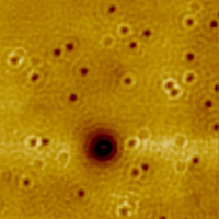
16 Oct 07:53
by Sangmo Cheon
Authors: Sangmo Cheon, Tae-Hwan Kim, Sung-Hoon Lee, Han Woong Yeom
14 Oct 11:02
by Nadine Hauptmann, César González, Fabian Mohn, Leo Gross, Gerhard Meyer and Richard Berndt
##IMG## [http://ej.iop.org/images/0957-4484/26/44/445703/nano519826ieqn1.gif] {${{\rm{C}}}_{60}$}
-functionalized tips are used to probe ##IMG##
[http://ej.iop.org/images/0957-4484/26/44/445703/nano519826ieqn2.gif] {${{\rm{C}}}_{60}$} molecules
on Cu(111) with scanning tunneling and atomic force microscopy. Distinct and complex intramolecular
contrasts are found. Maximal attractive forces are observed when for both molecules a [6,6] bond
faces a hexagon of the other molecule. Density functional theory calculations including
parameterized van der Waals interactions corroborate the observations.
12 Oct 07:41
by Ben Warner, Fadi El Hallak, Henning Prüser, John Sharp, Mats Persson, Andrew J. Fisher, Cyrus F. Hirjibehedin
Phenomena that are highly sensitive to magnetic fields can be exploited in
sensors and non-volatile memories. The scaling of such phenomena down to the
single molecule level may enable novel spintronic devices. Here we report
magnetoresistance in a single molecule junction arising from negative
differential resistance that shifts in a magnetic field at a rate two orders of
magnitude larger than Zeeman shifts. This sensitivity to the magnetic field
produces two voltage-tunable forms of magnetoresistance, which can be selected
via the applied bias. The negative differential resistance is caused by
transient charging of an iron phthalocyanine (FePc) molecule on a single layer
of copper nitride (Cu2N) on a Cu(001) surface, and occurs at voltages
corresponding to the alignment of sharp resonances in the filled and empty
molecular states with the Cu(001) Fermi energy. An asymmetric voltage-divider
effect enhances the apparent voltage shift of the negative differential
resistance with magnetic field, which inherently is on the scale of the Zeeman
energy. These results illustrate the impact that asymmetric coupling to
metallic electrodes can have on transport through molecules, and highlight how
this coupling can be used to develop molecular spintronic applications.
25 Sep 11:23
by Matthew Yankowitz, Devin McKenzie, and Brian J. LeRoy
Author(s): Matthew Yankowitz, Devin McKenzie, and Brian J. LeRoy
Tunneling spectroscopy exhibits suppression of intervalley electronic scattering in the valence band of a monolayer of the transition metal dichalcogenide WSe2.
[Phys. Rev. Lett. 115, 136803] Published Thu Sep 24, 2015
24 Sep 11:12
by D. Jacob, J. Fernández-Rossier
Quantum spin tunneling (QST) and Kondo effect are two very different quantum
phenomena that produce the same effect on quantized spins, namely, the
quenching of their magnetization. However, the nature of this quenching is very
different so that QST and Kondo effects compete with each other. Importantly,
both QST and Kondo produce very characteristic features in the spectral
function that can be measured by means of single spin scanning tunneling
spectroscopy that makes it possible to probe the crossover from one regime to
the other. We model this crossover, and the resulting changes in transport,
using a non-perturbative treatment of a generalized Anderson model including
magnetic anisotropy that leads to quantum spin tunneling. We predict that, at
zero magnetic field, integer spins can feature a split-Kondo peak driven by
quantum spin tunneling.
24 Sep 11:00
by Signe S. Grønborg, Søren Ulstrup, Marco Bianchi, Maciej Dendzik, Charlotte E. Sanders, Jeppe V. Lauritsen, Philip Hofmann, Jill A. Miwa
We present a method for synthesizing large area epitaxial single-layer
MoS$_2$ on the Au(111) surface in ultrahigh vacuum. Using scanning tunneling
microscopy and low energy electron diffraction, the evolution of the growth is
followed from nanoscale single-layer MoS$_2$ islands to a continuous MoS$_2$
layer. An exceptionally good control over the MoS$_2$ coverage is maintained
using an approach based on cycles of Mo evaporation and sulfurization to first
nucleate the MoS$_2$ nano-islands and then gradually increase their size.
During this growth process the native herringbone reconstruction of Au(111) is
lifted as shown by low energy electron diffraction measurements. Within these
MoS$_2$ islands, we identify domains rotated by 60$^{\circ}$ that lead to
atomically sharp line defects at domain boundaries. As the MoS$_2$ coverage
approaches the limit of a complete single-layer, the formation of bilayer
MoS$_2$ islands is initiated. Angle-resolved photoemission spectroscopy
measurements of both single and bilayer MoS$_2$ samples show a dramatic change
in their band structure around the center of the Brillouin zone. Brief exposure
to air after removing the MoS$_2$ layer from vacuum is not found to affect its
quality.
24 Sep 11:00
by Dongzhe Li, Cyrille Barreteau, Seiji Leo Kawahara, Jérôme Lagoute, Cyril Chacon, Yann Girard, Sylvie Rousset, Vincent Repain, Alexander Smogunov
The understanding of orbital hybridization and spin-polarization at the
organic-ferromagnetic interface is essential in the search for efficient hybrid
spintronic devices. Here, using first-principles calculations, we report a
systematic study of spin-split hybrid states of C$_{60}$ deposited on various
ferromagnetic surfaces: bcc-Cr(001), bcc-Fe(001), bcc-Co(001), fcc-Co(001) and
hcp-Co(0001). We show that the adsorption geometry of the molecule with respect
to the surface crystallographic orientation of the magnetic substrate as well
as the strength of the interaction play an intricate role in the
spin-polarization of the hybrid orbitals. We find that a large
spin-polarization in vacuum above the buckyball can only be achieved if the
molecule is adsorbed upon a bcc-(001) surface by its pentagonal ring. Therefore
bcc-Cr(001), bcc-Fe(001) and bcc-Co(001) are the optimal candidates.
Spin-polarized scanning tunneling spectroscopy measurements on single C$_{60}$
adsorbed on Cr(001) and Co/Pt(111) also confirm that both the symmetry of the
substrate and of the molecular conformation have a strong influence on the
induced spin polarization. Our finding may give valuable insights for further
engineering of spin filtering devices through single molecular orbitals.
Donate to arXiv
23 Sep 08:54
by Sahana Rößler, Cevriye Koz, Lin Jiao, Ulrich K. Rößler, Frank Steglich, Ulrich Schwarz, Steffen Wirth
The structurally simplest Fe-based superconductor FeSe with a critical
temperature $T_{c}\approx$ 8.5 K displays a breaking of the four-fold
rotational symmetry at a temperature $T_{s}\approx 87$ K. We investigated the
electronic properties of FeSe using scanning tunneling microscopy/spectroscopy
(STM/S), magnetization, and electrical transport measurements. The results
indicated two new energy scales (i) $T^{*} \approx$ 75 K denoted by an onset of
electron-hole asymmetry in STS, enhanced spin fluctuations, and increased
positive magnetoresistance; (ii) $T^{**} \approx$ 22 - 30 K, marked by opening
up of a partial gap of about 8 meV in STS and a recovery of Kohler's rule. Our
results reveal onset of an incipient ordering mode at $T^{*}$ and its
nucleation below $T^{**}$. The ordering mode observed here, both in spin as
well as charge channels, suggests a coupling between the spins with charge,
orbital or pocket degrees of freedom.
23 Sep 08:52
by Bart Ludbrook, Giorgio Levy, Pascal Nigge, Marta Zonno, Michael Schneider, David Dvorak, Christian Veenstra, Sergey Zhdanovich, Douglas Wong, Pinder Dosanjh, Carola Straßer, Alexander Stohr, Stiven Forti, Christian Ast, Ulrich Starke, Andrea Damascelli
Monolayer graphene exhibits many spectacular electronic properties, with
superconductivity being arguably the most notable exception. It was
theoretically proposed that superconductivity might be induced by enhancing the
electron-phonon coupling through the decoration of graphene with an alkali
adatom superlattice [Profeta et al. Nat. Phys. 8, 131-134 (2012)]. While
experiments have indeed demonstrated an adatom-induced enhancement of the
electron-phonon coupling, superconductivity has never been observed. Using
angle-resolved photoemission spectroscopy (ARPES) we show that lithium
deposited on graphene at low temperature strongly modifies the phonon density
of states, leading to an enhancement of the electron-phonon coupling of up to
$\lambda\!\simeq\!0.58$. On part of the graphene-derived $\pi^*$-band Fermi
surface, we then observe the opening of a $\Delta\!\simeq\!0.9$ meV
temperature-dependent pairing gap. This suggests, for the first time, that
Li-decorated monolayer graphene is superconducting at 3.5 K.
23 Sep 08:51
by Yoichi Miyahara, Jessica Topple, Zeno Schumacher, Peter Grutter
We report a new experimental technique for Kelvin probe force microscopy
(KPFM) using the dissipation signal of frequency modulation atomic force
microscopy for bias voltage feedback. It features a simple implementation and
faster scanning as it requires no low frequency modulation. The dissipation is
caused by the oscillating electrostatic force that is coherent with the tip
oscillation, which is induced by a sinusoidally oscillating voltage applied
between the tip and sample. We analyzed the effect of the phase of the
oscillating force on the frequency shift and dissipation and found that the
relative phase of 90$^\circ$ that causes only the dissipation is the most
appropriate for KPFM measurements. The present technique requires a
significantly smaller ac voltage amplitude by virtue of enhanced force
detection due to the resonance enhancement and the use of fundamental flexural
mode oscillation for electrostatic force detection. This feature will be of
great importance in the electrical characterizations of technically relevant
materials whose electrical properties are influenced by the externally applied
electric field as is the case in semiconductor electronic devices.
23 Sep 06:47
by Chenjia Tang, Chong Liu, Guanyu Zhou, Fangsen Li, Ding Zhang, Zheng Li, Canli Song, Shuaihua Ji, Ke He, Xi Chen, Lili Wang, Xucun Ma, Qi-Kun Xue
Alkali-metal (potassium) adsorption on FeSe thin films with thickness from
two unit cells (UC) to 4-UC on SrTiO3 grown by molecular beam epitaxy is
investigated with a low-temperature scanning tunneling microscope. At
appropriate potassium coverage (0.2-0.3 monolayer), the tunneling spectra of
the films all exhibit a superconducting-like gap larger than 11 meV (five times
the gap value of bulk FeSe), and two distinct features of characteristic phonon
modes at 11 meV and 21 meV. The results reveal the critical role of the
interface enhanced electron-phonon coupling for possible high temperature
superconductivity in the system and is consistent with recent theories. Our
study provides compelling evidence for the conventional pairing mechanism for
this type of heterostructure superconducting systems.
21 Sep 19:39
by Jinhai Mao, Yuhang Jiang, Dean Moldovan, Guohong Li, Kenji Watanabe, Takashi Taniguchi, Massoud Ramezani Masir, Francois M. Peeters, Eva Y. Andrei
The remarkable electronic properties of graphene have fueled the vision of a
graphene-based platform for lighter, faster and smarter electronics and
computing applications. One of the challenges is to devise ways to tailor its
electronic properties and to control its charge carriers. Here we show that a
single atom vacancy in graphene can stably host a local charge and that this
charge can be gradually built up by applying voltage pulses with the tip of a
scanning tunneling microscope (STM). The response of the conduction electrons
in graphene to the local charge is monitored with scanning tunneling and Landau
level spectroscopy, and compared to numerical simulations. As the charge is
increased, its interaction with the conduction electrons undergoes a transition
into a supercritical regime 6-11 where itinerant electrons are trapped in a
sequence of quasi-bound states which resemble an artificial atom. The
quasi-bound electron states are detected by a strong enhancement of the density
of states (DOS) within a disc centered on the vacancy site which is surrounded
by halo of hole states. We further show that the quasi-bound states at the
vacancy site are gate tunable and that the trapping mechanism can be turned on
and off, providing a new mechanism to control and guide electrons in graphene
21 Sep 17:37
by Katharina Höfer, Christoph Becker, Steffen Wirth, Liu Hao Tjeng
We have identified epitaxially grown elemental Te as a capping material that
is suited to protect the topological surface states of intrinsically insulating
Bi$_2$Te$_3$. By using angle-resolved photoemission, we were able to show that
the Te overlayer leaves the dispersive bands of the surface states intact and
that it does not alter the chemical potential of the Bi$_2$Te$_3$ thin film.
From in-situ four-point contact measurements, we observed that the conductivity
of the capped film is still mainly determined by the metallic surface states
and that the contribution of the capping layer is minor. Moreover, the Te
overlayer can be annealed away in vacuum to produce a clean Bi$_2$Te$_3$
surface in its pristine state even after the exposure of the capped film to
air. Our findings will facilitate well-defined and reliable ex-situ experiments
on the properties of Bi$_2$Te$_3$ surface states with nontrivial topology.
20 Sep 09:50
by Nuala M. Caffrey, Kristof Buchmann, Nadine Hauptmann, Cesar Lazo, Paolo Ferriani, Stefan Heinze and Richard Berndt

Nano Letters
DOI: 10.1021/acs.nanolett.5b01383

20 Sep 09:49
by Antonija Grubišić Čabo, Jill A. Miwa, Signe S. Grønborg, Jonathon M. Riley, Jens C. Johannsen, Cephise Cacho, Oliver Alexander, Richard T. Chapman, Emma Springate, Marco Grioni, Jeppe V. Lauritsen, Phil D. C. King, Philip Hofmann and Søren Ulstrup

Nano Letters
DOI: 10.1021/acs.nanolett.5b01967

20 Sep 09:48
by Nicholas Tallarida, Laura Rios, Vartkess A. Apkarian and Joonhee Lee

Nano Letters
DOI: 10.1021/acs.nanolett.5b01543

20 Sep 09:44
by J. M. Pereira, Jr. and M. I. Katsnelson
Author(s): J. M. Pereira, Jr. and M. I. Katsnelson
In this work we introduce a low-energy Hamiltonian for single-layer and bilayer black phosphorus that describes the electronic states at the vicinity of the Γ point. The model is based on a recently proposed tight-binding description for electron and hole bands close to the Fermi level. We calculate…
[Phys. Rev. B 92, 075437] Published Mon Aug 24, 2015
20 Sep 09:43
by Roland Bliem, Jiri Pavelec, Oscar Gamba, Eamon McDermott, Zhiming Wang, Stefan Gerhold, Margareta Wagner, Jacek Osiecki, Karina Schulte, Michael Schmid, Peter Blaha, Ulrike Diebold, and Gareth S. Parkinson
Author(s): Roland Bliem, Jiri Pavelec, Oscar Gamba, Eamon McDermott, Zhiming Wang, Stefan Gerhold, Margareta Wagner, Jacek Osiecki, Karina Schulte, Michael Schmid, Peter Blaha, Ulrike Diebold, and Gareth S. Parkinson
The adsorption of Ni, Co, Mn, Ti, and Zr at the (2×2)R45∘-reconstructed Fe3O4(001) surface was studied by scanning tunneling microscopy, x-ray and ultraviolet photoelectron spectroscopy, low-energy electron diffraction (LEED), and density functional theory (DFT). Following deposition at room tempera…
[Phys. Rev. B 92, 075440] Published Wed Aug 26, 2015
19 Sep 18:52
by W. Li, Y. Zhang, J. J. Lee, H. Ding, M. Yi, Z. Li, P. Deng, K. Chang, S.-K. Mo, M. Hashimoto, D. H. Lu, X. Chen, R. G. Moore, Q.-K. Xue, Z.-X. Shen
The intriguing role of nematicity in iron-based superconductors, defined as
broken rotational symmetry below a characteristic temperature, is an intensely
investigated contemporary subject. Nematicity is closely connected to the
structural transition, however, it is highly doubtful that the lattice degree
of freedom is responsible for its formation, given the accumulating evidence
for the observed large anisotropy. Here we combine molecular beam epitaxy,
angle-resolved photoemission spectroscopy and scanning tunneling microscopy
together to study the nematicity in multilayer FeSe films on SrTiO3. Our
results demonstrate direct connection between electronic anisotropy in momentum
space and standing waves in real space at atomic scale. The lifting of orbital
degeneracy of dxz/dyz bands gives rise to a pair of Dirac cone structures near
the zone corner, which causes energy-independent unidirectional interference
fringes, observed in real space as standing waves by scattering electrons off
C2 domain walls and Se-defects. On the other hand, the formation of C2 nematic
domain walls unexpectedly shows no correlation with lattice strain pattern,
which is induced by the lattice mismatch between the film and substrate. Our
results establish a clean case that the nematicity is driven by electronic
rather than lattice degrees of freedom in FeSe films.
19 Sep 18:49
by J. Fransson
Inelastic scattering off magnetic impurities in a spin-chiral two-dimensional
electron gas, e.g., the Rashba system, is shown to generate topological changes
in the spin texture of the electron waves emanating from the scattering center.
While elastic scattering gives rise to a purely in-plane spin texture for an
in-plane magnetic scat- tering potential, out-of-plane components emerge upon
activation of inelastic scattering processes. This property leads to a
possibility to make controlled transitions between trivial and nontrivial
topologies of the spin texture.
18 Sep 16:51
by Sebastian Frank, David Jacob
We investigate the orbital origin of the Fano-Kondo line shapes measured in
STM spectroscopy of magnetic adatoms on metal substrates. To this end we
calculate the low-bias tunnel spectra of a Co adatom on the (001) and (111) Cu
surfaces with our density functional theory-based ab initio transport scheme
augmented by local correlations. In order to associate different $d$-orbitals
with different Fano line shapes we only correlate individual $3d$-orbitals
instead of the full Co $3d$-shell. We find that Kondo peaks arising in
different $d$-levels indeed give rise to different Fano features in the
conductance spectra. Hence the shape of measured Fano features allows to draw
some conclusions about the orbital responsible for the Kondo resonance,
although the actual shape is also influenced by temperature, effective
interaction and charge fluctuations. Comparison with a simplified model shows
that line shapes are mostly the result of interference between tunneling paths
through the correlated $d$-orbital and the $sp$-type orbitals on the Co atom.
Very importantly, the amplitudes of the Fano features vary strongly among
orbitals, with the $3z^2$-orbital featuring by far the largest amplitude due to
its strong direct coupling to the $s$-type conduction electrons.
Donate to arXiv
18 Sep 16:48
by T. Thonhauser, S. Zuluaga, C. A. Arter, K. Berland, E. Schröder, P. Hyldgaard
We develop a proper nonempirical spin-density formalism for the van der Waals
density functional (vdW-DF) method. We show that this generalization, termed
svdW-DF, is firmly rooted in the single-particle nature of exchange and we test
it on a range of spin systems. We investigate in detail the role of spin in the
nonlocal-correlation driven adsorption of H$_2$ and CO$_2$ in the linear
magnets Mn-MOF74, Fe-MOF74, Co-MOF74, and Ni-MOF74. In all cases, we find that
spin plays a significant role during the adsorption process despite the general
weakness of the molecular-magnetic responses. The case of CO$_2$ adsorption in
Ni-MOF74 is particularly interesting, as the inclusion of spin effects results
in an increased attraction, opposite to what the diamagnetic nature of CO$_2$
would suggest. We explain this counter-intuitive result, tracking the behavior
to a coincidental hybridization of the O $p$ states with the Ni $d$ states in
the down-spin channel. More generally, by providing insight on nonlocal
correlation in concert with spin effects, our nonempirical svdW-DF method opens
the door for a deeper understanding of weak nonlocal magnetic interactions.
18 Sep 16:44
by A. Spinelli, M. Gerrits, R. Toskovic, B. Bryant, M. Ternes, A. F. Otte
A system of two exchange-coupled Kondo impurities in a magnetic field gives
rise to a rich phase space hosting a multitude of correlated phenomena.
Magnetic atoms on surfaces probed through scanning tunnelling microscopy
provide an excellent platform to investigate coupled impurities, but typical
high Kondo temperatures prevent field-dependent studies from being performed,
rendering large parts of the phase space inaccessible. We present an integral
study of pairs of Co atoms on insulating Cu2N/Cu(100), which each have a Kondo
temperature of only 2.6 K. In order to cover the different regions of the phase
space, the pairs are designed to have interaction strengths similar to the
Kondo temperature. By applying a sufficiently strong magnetic field, we are
able to access a new phase in which the two coupled impurities are
simultaneously screened. Comparison of differential conductance spectra taken
on the atoms to simulated curves, calculated using a third order transport
model, allows us to independently determine the degree of Kondo screening in
each phase.
18 Sep 16:41
by Maciej Dendzik, Matteo Michiardi, Charlotte Sanders, Marco Bianchi, Jill A. Miwa, Signe S. Grønborg, Jeppe Vang Lauritsen, Philip Hofmann
Large-area single-layer WS$_2$ is grown epitaxially on Au(111) using
evaporation of W atoms in a low pressure H$_2$S atmosphere. It is characterized
by means of scanning tunneling microscopy, low-energy electron diffraction and
core-level spectroscopy. Its electronic band structure is determined by
angle-resolved photoemission spectroscopy. The valence band maximum at
$\bar{K}$ is found to be significantly higher than at $\bar{\Gamma}$. The
observed dispersion around $\bar{K}$ is in good agreement with density
functional theory calculations for a free-standing monolayer, whereas the bands
at $\bar{\Gamma}$ are found to be hybridized with states originating from the
Au substrate. Strong spin-orbit coupling leads to a large spin-splitting of the
bands in the neighborhood of the $\bar{K}$ points, with a maximum splitting of
419(11)~meV. The valence band dispersion around $\bar{K}$ is found to be highly
anisotropic with spin-branch dependent effective hole masses of $0.40(02)m_e$
and $0.57(09)m_e$ for the upper and lower split valence band, respectively. The
large size of the spin-splitting and the low effective mass of the valence band
maximum make single-layer WS$_2$ a promising alternative to the widely studied
MoS$_2$ for applications in electronics, spintronics and valleytronics.
15 Sep 16:26
by Benjamin Bryant, Ranko Toskovic, Alejandro Ferrón, José L. Lado, Anna Spinelli, Joaquín Fernández-Rossier and Alexander F. Otte

Nano Letters
DOI: 10.1021/acs.nanolett.5b02200

09 Sep 07:47
by Michael Ruby, Falko Pientka, Yang Peng, Felix von Oppen, Benjamin W. Heinrich, and Katharina J. Franke
Author(s): Michael Ruby, Falko Pientka, Yang Peng, Felix von Oppen, Benjamin W. Heinrich, and Katharina J. Franke
We combine scanning-tunneling-spectroscopy experiments probing magnetic impurities on a superconducting surface with a theoretical analysis of the tunneling processes between (superconducting) tip and substrate. We show that the current through impurity-induced Shiba bound states is carried by singl…
[Phys. Rev. Lett. 115, 087001] Published Thu Aug 20, 2015
09 Sep 07:40
by Q. Fan
Nature Physics.
doi:10.1038/nphys3450
Authors: Q. Fan, W. H. Zhang, X. Liu, Y. J. Yan, M. Q. Ren, R. Peng, H. C. Xu, B. P. Xie, J. P. Hu, T. Zhang & D. L. Feng

09 Sep 07:39
by Xiaoxiang Xi
Nature Nanotechnology 10, 765 (2015).
doi:10.1038/nnano.2015.143
Authors: Xiaoxiang Xi, Liang Zhao, Zefang Wang, Helmuth Berger, László Forró, Jie Shan & Kin Fai Mak
Two-dimensional materials possess very different properties from their bulk counterparts. While changes in single-particle electronic properties have been investigated extensively, modifications in the many-body collective phenomena in the exact two-dimensional limit remain relatively unexplored. Here, we report a combined optical and electrical transport study on the many-body collective-order phase diagram of NbSe2 down to a thickness of one monolayer. Both the charge density wave and the superconducting phase have been observed down to the monolayer limit. The superconducting transition temperature decreases on lowering the layer thickness, but the newly observed charge-density-wave transition temperature increases from 33 K in the bulk to 145 K in the monolayer. Such highly unusual enhancement of charge density waves in atomically thin samples can be understood to be a result of significantly enhanced electron–phonon interactions in two-dimensional NbSe2 (ref. 4) and is supported by the large blueshift of the collective amplitude vibration observed in our experiment. Our results open up a new window for search and control of collective phases of two-dimensional matter, as well as expanding the functionalities of these materials for electronic applications.

30 Jul 19:27
by Ming-Yang Li
Two-dimensional transition metal dichalcogenides (TMDCs) such as molybdenum sulfide MoS2 and tungsten sulfide WSe2 have potential applications in electronics because they exhibit high on-off current ratios and distinctive electro-optical properties. Spatially connected TMDC lateral heterojunctions are key components for constructing monolayer p-n rectifying diodes, light-emitting diodes, photovoltaic devices, and bipolar junction transistors. However, such structures are not readily prepared via the layer-stacking techniques, and direct growth favors the thermodynamically preferred TMDC alloys. We report the two-step epitaxial growth of lateral WSe2-MoS2 heterojunction, where the edge of WSe2 induces the epitaxial MoS2 growth despite a large lattice mismatch. The epitaxial growth process offers a controllable method to obtain lateral heterojunction with an atomically sharp interface.
Authors: Ming-Yang Li, Yumeng Shi, Chia-Chin Cheng, Li-Syuan Lu, Yung-Chang Lin, Hao-Lin Tang, Meng-Lin Tsai, Chih-Wei Chu, Kung-Hwa Wei, Jr-Hau He, Wen-Hao Chang, Kazu Suenaga, Lain-Jong Li

