ACS Applied Materials & Interfaces
DOI: 10.1021/acsami.6b02169

By creating an effective π-orbital hybridization between the fullerene cage and the aromatic anchor (addend), the azafulleroid interfacial modifiers exhibit enhanced electronic coupling to the underneath metal oxides. High power conversion efficiency of 10.3% can be achieved in organic solar cells using open-cage phenyl C61 butyric acid methyl ester (PCBM)-modified zinc oxide layer.

A new approach is presented to control the nanomorphology of organic solar cells in a predictable, controllable, and easily-scalable way. The nanoimprint lithography (NIL) is combined with a subsequent molecular diffusion step controlled by thermal annealing. The new approach is realized by using nanointerdigitated donor–acceptor structure, consisting of poly(3-hexylthiophene-2,5-diyl) nanopillar arrays surrounded by phenyl-C61-butyric acid methyl ester. Subsequent thermal annealing leads to vertically aligned ordered quasi-bulk heterojunctions with hierarchical nanostructure. The changes are studied in nanostructural and electrical properties of the pillar samples using scanning probe microscopy. In addition, grazing-incidence small and wide angle X-ray scattering yield detailed quantitative information on the molecular- to domain-scale nanostructures. The changes in crystal size, chain orientation, and domain composition as a function of thermal anneal temperature and time are obtained. In addition, the conductive scanning force microscopy in quantitative imaging mode, applied to the pillar-based samples for the first time, allows us to establish a clear relationship between nanomorphology, nanoelectrical property, and macroscale device performance. It is believed that the NIL combined with controlled molecular diffusion is a powerful method, which could be easily extended to other materials and processes to realize a whole variety of other hierarchical nanomorphologies.

With controlled mutual diffusion of donor and acceptor molecules on well-defined nanointerdigitated donor–acceptor pillar structure, quasi-bulk heterojunction pillars are formed in large area. The pillar nanostructures are effectively controlled by varying the thermal annealing conditions, showing nano- to macroscale structural and electrical properties easily monitored by grazing-incidence X-ray scattering, and scanning force microscopy.

Photovoltaic (PV) infrared (IR)-based devices are important for a variety of industrial and scientific applications, such as IR imaging, biological sensing, day–night surveillance and in solar cells. However, most high-end IR PV devices made of conventional semiconductors need to be cooled to achieve high performance, while these materials usually are also not stable under strong illumination. Carbon nanotubes (CNTs) are direct-bandgap materials with a broad spectral response and a large absorption coefficient, which is most desired for building high-performance PV devices. Main progresses on CNT PVs in the past 15 years is reviewed, emphasizing recent breakthrough of CNT IR photodetectors based on solution-processed high-purity CNT films via a doping-free fabrication technique. This technique has been combined with virtual contacts to multiply the photovoltage and thus to significantly improve detection performance and signal-to-noise ratio of PV detectors. It is demonstrated that this CNT PV detector has a superior broadband response from visible to near-infrared light, high room-temperature detectivity comparable with state-of-the-art InGaAs detectors, and extremely good temperature and temporal stability. Challenges that still lay ahead and possible solutions are discussed.

The development of carbon nanotubes (CNT) photovoltaics with an emphasis on recent breakthroughs is reviewed. CNT IR (infrared) cascading photodetectors, based on high-purity solution-processed CNT films via the doping-free technique, exhibit a superior broadband response from visible to near-infrared, high room-temperature detectivity comparable to state-of-the-art InGaAs detectors, and extremely good temperature and temporal stability.
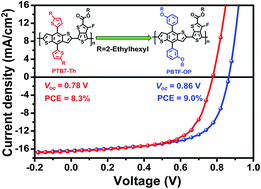
By the introduction of different building blocks and side-chains, a series of donor–acceptor type polymer acceptors containing naphthalene diimide have been successfully prepared. The theoretical and experimental results show that the molecular design effectively tunes the energy levels, solubility, and coplanarity of the acceptor polymers. The intermolecular packing, which has been considered as a key factor in the bulk heterojunction morphology, has been adjusted by changing the coplanarity. As a result of improved morphology and fine-tuned energy levels, a power conversion efficiency of 6.0% has been demonstrated for the optimized devices, which is among the highest-efficiencies for reported all-polymer solar cells. The improved device performance may be attributed to the resemble crystallinity of the donor/acceptor polymers, which can lead to the optimal phase separation morphology balancing both charge transfer and transport.

By incorporating different building blocks and modifying side-chains, a series of donor–acceptor polymers have been successfully synthesized. Optimized all-polymer solar cells have been demonstrated a high power conversion efficiency of 6.0%. The improved device performance may be attributed to the resemble crystallinity of the donor/acceptor polymers, which can lead to the balanced charge transfer and transport.
Carrier dynamics in methylammonium lead halide (CH3NH3PbI3–xClx) perovskite thin films, of differing crystal morphology, are examined as functions of temperature and excitation wavelength. At room temperature, long-lived (>nanosecond) transient absorption signals indicate negligible carrier trapping. However, in measurements of ultrafast photoluminescence excited at 400 nm, a heretofore unexplained, large amplitude (50%–60%), 45 ps decay process is observed. This feature persists for temperatures down to the orthorhombic phase transition. Varying pump photon energy reveals that the fast, band-edge photoluminescence (PL) decay only appears for excitation ≥2.38 eV (520 nm), with larger amplitudes for higher pump energies. Lower photon-energy excitation yields slow dynamics consistent with negligible carrier trapping. Further, sub-bandgap two-photon pumping yields identical PL dynamics as direct absorption, signifying sensitivity to the total deposited energy and insensitivity to interfacial effects. Together with first principles electronic structure and ab initio molecular dynamics calculations, the results suggest the fast PL decay stems from excitation of high energy phonon modes associated with the organic sub-lattice that temporarily enhance wavefunction overlap within the inorganic component owing to atomic displacement, thereby transiently changing the PL radiative rate during thermalization. Hence, the fast PL decay relates a characteristic organic-to-inorganic sub-lattice equilibration timescale at optoelectronic-relevant excitation energies.

Ultrafast photoluminescence dynamics in CH3NH3PbI3–xClx perovskite thin films are examined as functions of pump wavelength, temperature, and film morphology. A previously unexplained, rapid decay feature in emission, which occurs only for above-gap excitation and lacks thermal activation, arises from organic-to-inorganic thermalization of phonons. Density functional theory and transient mid-infrared spectroscopy further support the assignment of this important dissipation mechanism.

A perovskite LED with a perovskite film treated under optimum thermal annealing conditions exhibits a significantly enhanced long-term stability with full coverage of the green electroluminescence emission due to the highly uniform morphology of the perovskite film.

Organic–inorganic halide perovskite single crystals possess many outstanding properties conducive for photovoltaic and optoelectronic applications. However, a clear photophysics picture is still elusive, particularly, their surface and bulk photophysics are inexorably convoluted by the spectral absorbance, defects, coexisting photoexcited species, etc. In this work, an all-optical study is presented that clearly distinguishes the surface kinetics from those of the bulk in the representative methylammonium-lead bromide (MAPbBr3) and -lead iodide (MAPbI3) single crystals. It is found that the bulk recombination lifetime of the MAPbBr3 single crystal is shortened significantly by approximately one to two orders (i.e., from ≈34 to ≈1 ns) at the surface with a surface recombination velocity of around 6.7 × 103 cm s−1. The surface trap density is estimated to be around 6.0 × 1017 cm−3, which is two orders larger than that of the bulk (5.8 × 1015 cm−3). Correspondingly, the diffusion length of the surface excited species is ≈130–160 nm, which is considerably reduced compared to the bulk value of ≈2.6–4.3 μm. Furthermore, the surface region has a wider bandgap that possibly arises from the strong lattice deformation. The findings provide new insights into the intrinsic photophysics essential for single crystal perovskite photovoltaics and optoelectronic devices.

The surface and bulk photophysics of perovskite single crystals are clearly separated in an all-optical approach. Their surface photophysics is similar to that of polycrystalline thin films, but is significantly different in the bulk region. Key properties from both regions (e.g., recombination lifetimes, trap densities, surface recombination velocity, diffusion lengths, etc.) essential for optoelectronic applications are obtained in this comprehensive study.
During the past 6 years, perovskite solar cells have experienced a rapid development and shown great potential as the next-generation photovoltaics. For the perovskite solar cells with regular structure (n-i-p structure), device efficiency has reached over 20% after the intense efforts of researchers from all over the world. Recently, perovskite solar cells with the inverted structure (p-i-n structure) have been becoming more and more attractive, owing to their easy-fabrication, cost-effectiveness, and suppressed hysteresis characteristics. Some recent progress in their device performance and stability has indicated their promising future. Here, recent developments and future perspectives about inverted perovskite solar cells are reviewed. Interface engineering, film morphology control, device stability, hysteresis phenomena and other research hotspots are discussed to present the roadmap for the development of inverted perovskite solar cells.

Inverted perovskite solar cells are attracting much attention owing to their superior characteristics. Recent developments and future perspectives about inverted perovskite solar cells are reviewed. Interface engineering, film morphology control, device stability, hysteresis phenomena and other research hotspots are discussed to present the promising future of inverted perovskite solar cells.

The critical role of grain boundaries for (CH(NH2)2PbI3)0.85(CH3NH3PbBr3)0.15 perovskite solar cells studied by Kelvin probe force microscopy under bias voltage and illumination is reported. Ion migration is enhanced at the grain boundaries. Under illumination, the light-induced potential causes ion migration leading to a rearranged ion distribution. Such a distribution favors photogenerated charge-carrier collection at the grain boundaries.

All-vacuum-deposited perovskite solar cells produced by controlling reagent partial pressure in high vacuum with newly developed multi-layer electron and hole transporting structures show outstanding power conversion efficiency of 17.6% and smooth, pinhole-free, micrometer-sized perovskite crystal grains.
Organolead halide perovskites (e.g., CH3NH3PbI3) have caught tremendous attention for their excellent optoelectronic properties and applications, especially as the active material for solar cells. Perovskite crystal quality and dimension is crucial for the fabrication of high-performance optoelectronic and photovoltaic devices. Herein the controlled synthesis of organolead halide perovskite CH3NH3PbI3 nanoplatelets on SiO2/Si substrates is investigated via a convenient two-step vapor transport deposition technique. The thickness and size of the perovskite can be well-controlled from few-layers to hundred nanometers by altering the synthesis time and temperature. Raman characterizations reveal that the evolutions of Raman peaks are sensitive to the thickness. Furthermore, from the time-resolved photoluminescence measurements, the best optoelectronic performance of the perovskite platelet is attributed with thickness of ≈30 nm to its dominant longest lifetime (≈4.5 ns) of perovskite excitons, which means lower surface traps or defects. This work supplies an alternative to the synthesis of high-quality organic perovskite and their possible optoelectronic applications with the most suitable materials.

High-quality organic–inorganic perovskite nanoplatelets can be well-controlled synthesized from few-layers to hundred nanometers on Si/SiO2 substrate. Raman characterizations reveal that the evolutions of Raman peaks are sensitive to the thickness. Furthermore, under the thickness-dependent photoresponse and time-resolved photoluminescence measurements of perovskite devices, the results indicate the most suitable thickness for their possible optoelectronic applications.
Energy-related functionality and performance of organic–inorganic hybrid perovskites, such as methylammonium lead iodide (MAPbI3), highly depend on their thermal transport behavior. Using equilibrium molecular dynamics simulations, it is discovered that the thermal conductivities of MAPbI3 under different phases (cubic, tetragonal, and orthorhombic) are less than 1 W m−1 K−1, and as low as 0.31 W m−1 K−1 at room temperature. Such ultralow thermal conductivity can be attributed to the small phonon group velocities due to their low elastic stiffness, in addition to their short phonon lifetimes (<100 ps) and mean-free-paths (<10 nm) due to the enhanced phonon–phonon scattering from highly-overlapped phonon branches. The anisotropy in thermal conductivity at lower temperatures is found to associate with preferential orientations of organic CH3NH3+ cations. Among all atomistic interactions, electrostatic interactions dominate thermal conductivities in ionic MAPbI3 crystals. Furthermore, thermal conductivities of general hybrid perovskites MABX3 (B = Pb, Sn; X = I, Br) have been qualitatively estimated and found that Sn- or Br-based perovskites possess higher thermal conductivities than Pb- or I-based ones due to their much higher elastic stiffness. This study inspires optimal selections and rational designs of ionic components for hybrid perovskites with desired thermal conductivity for thermally-stable photovoltaic or highly-efficient thermoelectric energy harvesting/conversion applications.

The ultralow thermal conductivity of organic–inorganic perovskite (CH3NH3PbI3) (<1 W m−1 K−1) is demonstrated. Such ultralow conductivity results from small phonon group velocities and short phonon lifetimes. Furthermore, the optimal selections and rational designs of the ionic components for hybrid perovskites MABX3 (B = Pb, Sn; X = I, Br) are further discussed.
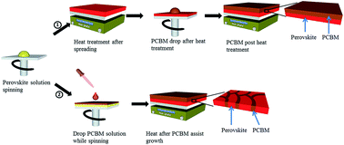
Grazing incidence wide and small angle X-ray scattering (GIWAXS and GISAXS) measurements have been used to study the crystallization kinetics of the organolead halide perovskite CH3NH3PbI3–xClx during thermal annealing. In situ GIWAXS measurements recorded during annealing are used to characterize and quantify the transition from a crystalline precursor to the perovskite structure. In situ GISAXS measurements indicate an evolution of crystallite sizes during annealing, with the number of crystallites having sizes between 30 and 400 nm increasing through the annealing process. Using ex situ scanning electron microscopy, this evolution in length scales is confirmed and a concurrent increase in film surface coverage is observed, a parameter crucial for efficient solar cell performance. A series of photovoltaic devices are then fabricated in which perovskite films have been annealed for different times, and variations in device performance are explained on the basis of X-ray scattering measurements.

Crystallization of the perovskite CH3NH3PbI3–xClx during thermal annealing of a precursor film is studied using in situ grazing incidence wide angle and small angle X-ray scattering measurements. These results can explain the evolution of device performance with annealing time, and optimized films lead to solar cells with average power conversion efficiencies of over 12%.