13 Jan 15:26
by Sabine Abb
Article
Peptide nanostructures are currently arousing interest thanks to their potential applications in medicine, electronics and coatings. Here, through experiment and theory, the authors demonstrate exquisite control over surface peptide assembly behaviour through manipulation of amino acid sequence.
Nature Communications doi: 10.1038/ncomms10335
Authors: Sabine Abb, Ludger Harnau, Rico Gutzler, Stephan Rauschenbach, Klaus Kern

13 Jan 02:30
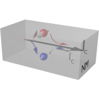
by Pin-Jui Hsu, André Kubetzka, Aurore Finco, Niklas Romming, Kirsten von Bergmann, Roland Wiesendanger
Controlling magnetism with electric fields is a key challenge to develop
future energy-efficient devices, however, the switching between inversion
symmetric states, e.g. magnetization up and down as used in current technology,
is not straightforward, since the electric field does not break time-reversal
symmetry. Here, we demonstrate that local electric fields can be used to
reversibly switch between a magnetic skyrmion and the ferromagnetic state.
These two states are topologically inequivalent, and we find that the direction
of an electric field directly determines the final state. This observation
establishes the possibility to combine energy-efficient electric field writing
with the recently envisaged skyrmion racetrack-type memories.
Donate to arXiv
13 Jan 02:21
by Shichao Yan, Luigi Malavolti, Jacob A. J. Burgess, Sebastian Loth
The ability to sense the magnetic state of individual magnetic nano-objects
is a key capability for powerful applications ranging from readout of
ultra-dense magnetic memory to the measurement of spins in complex structures
with nanometer precision. Magnetic nano-objects require extremely sensitive
sensors and detection methods. Here we create an atomic spin sensor consisting
of three Fe atoms and show that it can detect nanoscale antiferromagnets
through minute surface-mediated magnetic interaction. Coupling, even to an
object with no net spin and having vanishing dipolar stray field, modifies the
transition matrix element between two spin states of the Fe-atom-based spin
sensor that changes the sensor's spin relaxation time. The sensor can detect
nanoscale antiferromagnets at up to three nanometers distance and achieves an
energy resolution of 10 micro-electronvolts surpassing the thermal limit of
conventional scanning probe spectroscopy. This scheme permits simultaneous
sensing of multiple antiferromagnets with a single spin sensor integrated onto
the surface.
13 Jan 01:30
by Hao Zheng, Su-Yang Xu, Guang Bian, Cheng Guo, Guoqing Chang, Daniel S. Sanchez, Ilya Belopolski, Chi-Cheng Lee, Shin-Ming Huang, Xiao Zhang, Raman Sankar, Nasser Alidoust, Tay-Rong Chang, Fan Wu, Titus Neupert, Fangcheng Chou, Horng-Tay Jeng, Nan Yao, Arun Bansil, Shuang Jia, Hsin Lin and M. Zahid Hasan

ACS Nano
DOI: 10.1021/acsnano.5b06807

13 Jan 00:48
by P. Sessi, O. Storz, T. Bathon, S. Wilfert, K. A. Kokh, O. E. Tereshchenko, G. Bihlmayer, and M. Bode
Author(s): P. Sessi, O. Storz, T. Bathon, S. Wilfert, K. A. Kokh, O. E. Tereshchenko, G. Bihlmayer, and M. Bode
The binary chalcogenides Bi2Te3 and Bi2Se3 are the most widely studied topological insulators. Although the quantum anomalous Hall effect has recently been observed in magnetically doped Sb2Te3, this compound has been studied to a much lesser extent. Here, by using energy-resolved quasiparticle inte…
[Phys. Rev. B 93, 035110] Published Tue Jan 12, 2016
12 Jan 21:16
by Jiaming Song, Matthias Bernien, Chii-Bin Wu and Wolfgang Kuch

The Journal of Physical Chemistry C
DOI: 10.1021/acs.jpcc.5b10017

12 Jan 14:05
by Eric Le Moal, Sylvie Marguet, Damien Canneson, Benoît Rogez, Elizabeth Boer-Duchemin, Gérald Dujardin, Tatiana V. Teperik, Dana-Codruta Marinica, and Andrey G. Borisov
Author(s): Eric Le Moal, Sylvie Marguet, Damien Canneson, Benoît Rogez, Elizabeth Boer-Duchemin, Gérald Dujardin, Tatiana V. Teperik, Dana-Codruta Marinica, and Andrey G. Borisov
The inelastic tunnel current in the junction formed between the tip of a scanning tunneling microscope (STM) and the sample can electrically generate optical signals. This phenomenon is potentially of great importance for nano-optoelectronic devices. In practice, however, the properties of the emitt…
[Phys. Rev. B 93, 035418] Published Mon Jan 11, 2016
09 Jan 17:07
by Kian Ping Loh, Shi Wun Tong and Jishan Wu

Journal of the American Chemical Society
DOI: 10.1021/jacs.5b10917

09 Jan 16:48
by Wen-Xiao Wang, Mei Zhou, Xinqi Li, Si-Yu Li, Xiaosong Wu, Wenhui Duan, Lin He
Graphene nanoribbons (GNRs) are one-dimensional (1D) structures that exhibit
a rich variety of electronic properties1-17. Therefore, they are predicted to
be the building blocks in next-generation nanoelectronic devices.
Theoretically, it has been demonstrated that armchair GNRs can be divided into
three families, i.e., Na = 3p, Na = 3p + 1, and Na = 3p + 2 (here Na is the
number of dimer lines across the ribbon width and p is an integer), according
to their electronic structures, and the energy gaps for the three families are
quite different even with the same p1,3-6. However, a systematic experimental
verification of this fundamental prediction is still lacking, owing to very
limited atomic-level control of the width of the armchair GNRs
investigated7,9,10,13,17. Here, we studied electronic structures of the
armchair GNRs with atomically well-defined widths ranging from Na = 6 to Na =
26 by using scanning tunnelling microscope (STM). Our result demonstrated
explicitly that all the studied armchair GNRs exhibit semiconducting gaps due
to quantum confinement and, more importantly, the observed gaps as a function
of Na are well grouped into the three categories, as predicted by
density-functional theory calculations3. Such a result indicated that we can
tune the electronic properties of the armchair GNRs dramatically by simply
adding or cutting one carbon dimer line along the ribbon width.
Donate to arXiv
09 Jan 16:37
by Saül Vélez, Vitaly N. Golovach, Amilcar Bedoya-Pinto, Miren Isasa, Edurne Sagasta, Mikel Abadia, Celia Rogero, Luis E. Hueso, F. Sebastian Bergeret, and Fèlix Casanova
Author(s): Saül Vélez, Vitaly N. Golovach, Amilcar Bedoya-Pinto, Miren Isasa, Edurne Sagasta, Mikel Abadia, Celia Rogero, Luis E. Hueso, F. Sebastian Bergeret, and Fèlix Casanova
A new type of magnetoresistance is measured in thin nonmagnetic platinum films with strong spin-orbit coupling due to spin accumulation at the surface of the film.
[Phys. Rev. Lett. 116, 016603] Published Fri Jan 08, 2016
09 Jan 16:34
by Fabian D. Natterer, Jeonghoon Ha, Hongwoo Baek, Duming Zhang, William G. Cullen, Nikolai B. Zhitenev, Young Kuk, and Joseph A. Stroscio
Author(s): Fabian D. Natterer, Jeonghoon Ha, Hongwoo Baek, Duming Zhang, William G. Cullen, Nikolai B. Zhitenev, Young Kuk, and Joseph A. Stroscio
We report on spatial measurements of the superconducting proximity effect in epitaxial graphene induced by a graphene-superconductor interface. Superconducting aluminum films were grown on epitaxial multilayer graphene on SiC. The aluminum films were discontinuous, with networks of trenches in the f…
[Phys. Rev. B 93, 045406] Published Thu Jan 07, 2016
09 Jan 16:33
by A. C. Garcia-Castro, M. G. Vergniory, E. Bousquet, and A. H. Romero
Author(s): A. C. Garcia-Castro, M. G. Vergniory, E. Bousquet, and A. H. Romero
The electronic structure of SrTiO3 and SrHfO3 (001) surfaces with oxygen vacancies is studied by means of first-principles calculations. We reveal how oxygen vacancies within the first atomic layer of the SrTiO3 surface (i) induce a large antiferrodistortive motion of the oxygen octahedra at the sur…
[Phys. Rev. B 93, 045405] Published Thu Jan 07, 2016
07 Jan 20:17
by Amanda E. Anderson, Federico Grillo, Christian R. Larrea, Riho T. Seljamäe-Green, Herbert A. Früchtl and Christopher J. Baddeley

The Journal of Physical Chemistry C
DOI: 10.1021/acs.jpcc.5b10489

07 Jan 16:44
by José A. Castro-Osma, Michael North, Xiao Wu
Abstract
Chromium and aluminium salphen complexes have been found to display remarkable catalytic activity in the synthesis of cyclic carbonates from a range of epoxides and carbon dioxide. The Al(salphen) complex is more reactive towards terminal epoxides at ambient temperature and pressure, whereas the Cr(salphen) complex exhibits higher catalytic activity towards more challenging internal epoxides at elevated temperature and pressure.

Have you got the metal for it? Diethylamino-substituted chromium and aluminium salphen complexes both catalyse the synthesis of cyclic carbonates from epoxides and carbon dioxide, but show different substrate preferences. The chromium complex is best for internal epoxides whilst the aluminium complex is best for terminal epoxides.
07 Jan 15:13
Phys. Chem. Chem. Phys., 2016, Advance Article
DOI: 10.1039/C5CP07320K, Paper
Osman Ahmed Zelekew, Dong-Hau Kuo
The mechanism for the reduction reaction of 4-nitrophenol to 4-aminophenol in the presence of a SiO2/Ag2O@TiO2 composite catalyst.
To cite this article before page numbers are assigned, use the DOI form of citation above.
The content of this RSS Feed (c) The Royal Society of Chemistry

07 Jan 11:36
by Toan Trong Tran
Nature Nanotechnology 11, 37 (2016).
doi:10.1038/nnano.2015.242
Authors: Toan Trong Tran, Kerem Bray, Michael J. Ford, Milos Toth & Igor Aharonovich
Artificial atomic systems in solids are widely considered the leading physical system for a variety of quantum technologies, including quantum communications, computing and metrology. To date, however, room-temperature quantum emitters have only been observed in wide-bandgap semiconductors such as diamond and silicon carbide, nanocrystal quantum dots, and most recently in carbon nanotubes. Single-photon emission from two-dimensional materials has been reported, but only at cryogenic temperatures. Here, we demonstrate room-temperature, polarized and ultrabright single-photon emission from a colour centre in two-dimensional hexagonal boron nitride. Density functional theory calculations indicate that vacancy-related defects are a probable source of the emission. Our results demonstrate the unprecedented potential of van der Waals crystals for large-scale nanophotonics and quantum information processing.

05 Jan 22:12
by Hyun-Jung Kim, Chaokai Li, Ji Feng, Jun-Hyung Cho, and Zhenyu Zhang
Author(s): Hyun-Jung Kim, Chaokai Li, Ji Feng, Jun-Hyung Cho, and Zhenyu Zhang
The exploration of topological states is of significant fundamental and practical importance in contemporary condensed matter physics, for which the extension to two-dimensional (2D) organometallic systems is particularly attractive. Using first-principles calculations, we show that a 2D hexagonal t…
[Phys. Rev. B 93, 041404(R)] Published Tue Jan 05, 2016
05 Jan 21:16
by Pin-Jui Hsu, Aurore Finco, Lorenz Schmidt, André Kubetzka, Kirsten von Bergmann, and Roland Wiesendanger
Author(s): Pin-Jui Hsu, Aurore Finco, Lorenz Schmidt, André Kubetzka, Kirsten von Bergmann, and Roland Wiesendanger
Nanometer cycloidal spin spirals are observed on strained double-layers of iron where the layers have different lattice orientations.
[Phys. Rev. Lett. 116, 017201] Published Tue Jan 05, 2016
05 Jan 10:02
by Albert Bruix, Jill A. Miwa, Nadine Hauptmann, Daniel Wegner, Søren Ulstrup, Signe S. Grønborg, Charlotte E. Sanders, Maciej Dendzik, Antonija Grubišić Čabo, Marco Bianchi, Jeppe V. Lauritsen, Alexander A. Khajetoorians, Bjørk Hammer, Philip Hofmann
The electronic structure of epitaxial single-layer MoS$_2$ on Au(111) is
investigated by angle-resolved photoemission spectroscopy, scanning tunnelling
spectroscopy, and first principles calculations. While the band dispersion of
the supported single-layer is close to a free-standing layer in the vicinity of
the valence band maximum at $\bar{K}$ and the calculated electronic band gap on
Au(111) is similar to that calculated for the free-standing layer, significant
modifications to the band structure are observed at other points of the
two-dimensional Brillouin zone: At $\bar{\Gamma}$, the valence band maximum has
a significantly higher binding energy than in the free MoS$_2$ layer and the
expected spin-degeneracy of the uppermost valence band at the $\bar{M}$ point
cannot be observed. These band structure changes are reproduced by the
calculations and can be explained by the detailed interaction of the
out-of-plane MoS$_2$ orbitals with the substrate.
Donate to arXiv
05 Jan 09:57
by Guillaume Vasseur
Article
Polymerization on surfaces is an emerging approach for producing graphene nanoribbons with a tunable bandgap, a promising material for carbon-based electronics. Here, Vasseur et al. show quasi-one-dimensional band structure of a model semiconducting polymer synthesized directly on a supporting surface.
Nature Communications doi: 10.1038/ncomms10235
Authors: Guillaume Vasseur, Yannick Fagot-Revurat, Muriel Sicot, Bertrand Kierren, Luc Moreau, Daniel Malterre, Luis Cardenas, Gianluca Galeotti, Josh Lipton-Duffin, Federico Rosei, Marco Di Giovannantonio, Giorgio Contini, Patrick Le Fèvre, François Bertran, Liangbo Liang, Vincent Meunier, Dmitrii F. Perepichka

04 Jan 21:16
by Wei Li, Wei-Guo Yin, Lili Wang, Ke He, Xucun Ma, Qi-Kun Xue, and Xi Chen
Author(s): Wei Li, Wei-Guo Yin, Lili Wang, Ke He, Xucun Ma, Qi-Kun Xue, and Xi Chen
We use scanning tunneling microscopy and spectroscopy to reveal a unique stripy charge order in a parent phase of iron-based superconductors in stoichiometric FeTe epitaxy films. The charge order has unusually the same—usually half—period as the spin order. We also found highly anisotropic electron …
[Phys. Rev. B 93, 041101(R)] Published Mon Jan 04, 2016
04 Jan 21:14
by Maciej Bazarnik, Bernhard Bugenhagen, Micha Elsebach, Emil Sierda, Annika Frank, Marc H. Prosenc and Roland Wiesendanger

Nano Letters
DOI: 10.1021/acs.nanolett.5b04266

29 Dec 21:06
by Hyo Won Kim, Seiji Takemoto, Emi Minamitani, Tomonari Okada, Takeshi Takami, Kenta Motobayashi, Michael Trenary, Maki Kawai, Nobuhiko Kobayashi and Yousoo Kim

The Journal of Physical Chemistry C
DOI: 10.1021/acs.jpcc.5b10040

28 Dec 19:00
by Maciej Dendzik, Matteo Michiardi, Charlotte Sanders, Marco Bianchi, Jill A. Miwa, Signe S. Grønborg, Jeppe V. Lauritsen, Albert Bruix, Bjørk Hammer, and Philip Hofmann
Author(s): Maciej Dendzik, Matteo Michiardi, Charlotte Sanders, Marco Bianchi, Jill A. Miwa, Signe S. Grønborg, Jeppe V. Lauritsen, Albert Bruix, Bjørk Hammer, and Philip Hofmann
Large-area single-layer WS2 is grown epitaxially on Au(111) using evaporation of W atoms in a low pressure H2S atmosphere. It is characterized by means of scanning tunneling microscopy, low-energy electron diffraction, and core level spectroscopy. Its electronic band structure is determined by angle…
[Phys. Rev. B 92, 245442] Published Mon Dec 28, 2015
28 Dec 18:59
by Florian Albrecht, Martin Fleischmann, Manfred Scheer, Leo Gross, and Jascha Repp
Author(s): Florian Albrecht, Martin Fleischmann, Manfred Scheer, Leo Gross, and Jascha Repp
In the past, current-distance spectroscopy has been widely applied to determine variations of the work function at surfaces. While for homogeneous sample areas this technique is commonly accepted to yield at least qualitative results, its applicability to atomic-scale variations has not been proven …
[Phys. Rev. B 92, 235443] Published Mon Dec 28, 2015
24 Dec 00:09
by Chen Sun
Single-chip microprocessor that communicates directly using light
Nature 528, 7583 (2015). doi:10.1038/nature16454
Authors: Chen Sun, Mark T. Wade, Yunsup Lee, Jason S. Orcutt, Luca Alloatti, Michael S. Georgas, Andrew S. Waterman, Jeffrey M. Shainline, Rimas R. Avizienis, Sen Lin, Benjamin R. Moss, Rajesh Kumar, Fabio Pavanello, Amir H. Atabaki, Henry M. Cook, Albert J. Ou, Jonathan C. Leu, Yu-Hsin Chen, Krste Asanović, Rajeev J. Ram, Miloš A. Popović & Vladimir M. Stojanović
Data transport across short electrical wires is limited by both bandwidth and power density, which creates a performance bottleneck for semiconductor microchips in modern computer systems—from mobile phones to large-scale data centres. These limitations can be overcome by using optical communications based on chip-scale electronic–photonic systems enabled by silicon-based nanophotonic devices8. However, combining electronics and photonics on the same chip has proved challenging, owing to microchip manufacturing conflicts between electronics and photonics. Consequently, current electronic–photonic chips are limited to niche manufacturing processes and include only a few optical devices alongside simple circuits. Here we report an electronic–photonic system on a single chip integrating over 70 million transistors and 850 photonic components that work together to provide logic, memory, and interconnect functions. This system is a realization of a microprocessor that uses on-chip photonic devices to directly communicate with other chips using light. To integrate electronics and photonics at the scale of a microprocessor chip, we adopt a ‘zero-change’ approach to the integration of photonics. Instead of developing a custom process to enable the fabrication of photonics, which would complicate or eliminate the possibility of integration with state-of-the-art transistors at large scale and at high yield, we design optical devices using a standard microelectronics foundry process that is used for modern microprocessors. This demonstration could represent the beginning of an era of chip-scale electronic–photonic systems with the potential to transform computing system architectures, enabling more powerful computers, from network infrastructure to data centres and supercomputers.

23 Dec 21:41
by Joost van der Lit, Jolien L. Marsman, Rik S. Koster, Peter H. Jacobse, Stephan A. den Hartog, Daniel Vanmaekelbergh, Robertus J. M. Klein Gebbink, Laura Filion and Ingmar Swart

The Journal of Physical Chemistry C
DOI: 10.1021/acs.jpcc.5b09889

23 Dec 21:38
by Albert C. Aragonès, Daniel Aravena, Jorge I. Cerdá, Zulema Acís-Castillo, Haipeng Li, José Antonio Real, Fausto Sanz, Josh Hihath, Eliseo Ruiz and Ismael Díez-Pérez

Nano Letters
DOI: 10.1021/acs.nanolett.5b03571

23 Dec 21:37
by K. Honma, T. Sato, S. Souma, K. Sugawara, Y. Tanaka, and T. Takahashi
Author(s): K. Honma, T. Sato, S. Souma, K. Sugawara, Y. Tanaka, and T. Takahashi
We have performed spin- and angle-resolved photoemission spectroscopy on tungsten (110) interfaced with an ultrathin iron (Fe) layer to study an influence of ferromagnetism on the Dirac-cone-like surface-interface states. We found an unexpectedly large energy gap of 340 meV at the Dirac point, and h…
[Phys. Rev. Lett. 115, 266401] Published Wed Dec 23, 2015
23 Dec 21:33
by Stefan Müllegger, Eva Rauls, Uwe Gerstmann, Stefano Tebi, Giulia Serrano, Stefan Wiespointner-Baumgarthuber, Wolf Gero Schmidt, and Reinhold Koch
Author(s): Stefan Müllegger, Eva Rauls, Uwe Gerstmann, Stefano Tebi, Giulia Serrano, Stefan Wiespointner-Baumgarthuber, Wolf Gero Schmidt, and Reinhold Koch
Recent radio frequency scanning tunneling spectroscopy (rf-STS) experiments have demonstrated nuclear and electron spin excitations up to ±12ℏ in a single molecular spin quantum dot (qudot). Despite the profound experimental evidence, the observed independence of the well-established dipole selectio…
[Phys. Rev. B 92, 220418(R)] Published Wed Dec 23, 2015


