08 Jul 02:10
Nanoscale, 2017, 9,9440-9446
DOI: 10.1039/C7NR01678F, Paper
John Ciro, Santiago Mesa, Jose Ignacio Uribe, Mario Alejandro Mejia-Escobar, Daniel Ramirez, Juan Felipe Montoya, Rafael Betancur, Hyun-Seok Yoo, Nam-Gyu Park, Franklin Jaramillo
Rhodamine interlayer reduces trap states at the PCBM surface while hindering moisture access.
The content of this RSS Feed (c) The Royal Society of Chemistry

08 Jul 02:10
by Adam D. Wright, Rebecca L. Milot, Giles E. Eperon, Henry J. Snaith, Michael B. Johnston, Laura M. Herz
Traps limit the photovoltaic efficiency and affect the charge transport of optoelectronic devices based on hybrid lead halide perovskites. Understanding the nature and energy scale of these trap states is therefore crucial for the development and optimization of solar cell and laser technology based on these materials. Here, the low-temperature photoluminescence of formamidinium lead triiodide (HC(NH2)2PbI3) is investigated. A power-law time dependence in the emission intensity and an additional low-energy emission peak that exhibits an anomalous relative Stokes shift are observed. Using a rate-equation model and a Monte Carlo simulation, it is revealed that both phenomena arise from an exponential trap-density tail with characteristic energy scale of ≈3 meV. Charge-carrier recombination from sites deep within the tail is found to cause emission with energy downshifted by up to several tens of meV. Hence, such phenomena may in part be responsible for open-circuit voltage losses commonly observed in these materials. In this high-quality hybrid perovskite, trap states thus predominantly comprise a continuum of energetic levels (associated with disorder) rather than discrete trap energy levels (associated, e.g., with elemental vacancies). Hybrid perovskites may therefore be viewed as classic semiconductors whose band-structure picture is moderated by a modest degree of energetic disorder.

Low-temperature measurements of the photoluminescence from HC(NH2)2PbI3 thin films are presented. The emission exhibits a power-law intensity decay with time after excitation, and an additional low-energy peak displaying an anomalous Stokes shift. These phenomena demonstrate that charge–carrier recombination in this perovskite is mediated by a band tail with characteristic energy 3 meV, determined from a rate-equation model and Monte Carlo simulation.
06 Jul 11:47
by Paolo Postorino and Lorenzo Malavasi

The Journal of Physical Chemistry Letters
DOI: 10.1021/acs.jpclett.7b00347

06 Jul 11:45
by Heping Shen, Daniel A. Jacobs, Yiliang Wu, The Duong, Jun Peng, Xiaoming Wen, Xiao Fu, Siva K. Karuturi, Thomas P. White, Klaus Weber and Kylie R. Catchpole

The Journal of Physical Chemistry Letters
DOI: 10.1021/acs.jpclett.7b00571

15 Jun 11:34
by Marina Freitag
Nature Photonics 11, 372 (2017).
doi:10.1038/nphoton.2017.60
Authors: Marina Freitag, Joël Teuscher, Yasemin Saygili, Xiaoyu Zhang, Fabrizio Giordano, Paul Liska, Jianli Hua, Shaik M. Zakeeruddin, Jacques-E. Moser, Michael Grätzel & Anders Hagfeldt

15 Jun 04:32
J. Mater. Chem. A, 2017, 5,13220-13227
DOI: 10.1039/C7TA02440A, Paper
Sang Jin Park, Seolhee Jeon, In Kyu Lee, Jing Zhang, Huiseong Jeong, Ji-Yong Park, Jiwon Bang, Tae Kyu Ahn, Hee-Won Shin, Bong-Gi Kim, Hui Joon Park
Triarylamine derivatives containing electron donating methoxy units provide outstanding device performance as dopant-free hole transporting materials in inverse type planar heterojunction perovskite solar cells.
The content of this RSS Feed (c) The Royal Society of Chemistry
15 Jun 04:31
J. Mater. Chem. A, 2017, 5,13145-13153
DOI: 10.1039/C7TA03472E, Paper
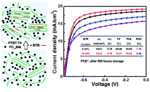
Xiaoling Ma, Fujun Zhang, Qiaoshi An, Qianqian Sun, Miao Zhang, Jianli Miao, Zhenghao Hu, Jian Zhang
BTR as a nucleating agent is incorporated into PTB7-Th:PC71BM to optimize their molecular arrangement and phase separation. The PCE and stability of the ternary PSCs are simultaneously improved due to the optimized morphology.
The content of this RSS Feed (c) The Royal Society of Chemistry
15 Jun 04:29
J. Mater. Chem. A, 2017, 5,13581-13590
DOI: 10.1039/C7TA02936E, Paper
Hee Uk Lee, Seung Wook Kim
An energy device using an all solid-state microsupercapacitor (MSC) has to play the roles of both a current collector and an electrode material, as well as demonstrating properties of high charge storage, conductivity, and flexibility.
The content of this RSS Feed (c) The Royal Society of Chemistry
15 Jun 04:28
J. Mater. Chem. A, 2017, 5,12416-12425
DOI: 10.1039/C7TA03150E, Paper
Yan-Zhen Zheng, Er-Fei Zhao, Fan-Li Meng, Xue-Sen Lai, Xue-Mei Dong, Jiao-Jiao Wu, Xia Tao
A compact and even ZnO:I nanopillar planar electron transport layer (ETL) is prepared to enable deposition of a fully covering and highly uniform perovskite layer by a facile one-step spin-coating process method. Such a ZnO:I nanopillar ETL film exhibits high optical transparency, favorable work function and superior electron extraction ability, leading to the opt-electrical conversion efficiency as high as 18.24%.
The content of this RSS Feed (c) The Royal Society of Chemistry
15 Jun 04:28
J. Mater. Chem. A, 2017, 5,13817-13822
DOI: 10.1039/C7TA02670F, Paper
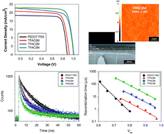
Ju Huang, Kai-Xuan Wang, Jing-Jing Chang, Yan-Yun Jiang, Qi-Shi Xiao, Yuan Li
Dopamine-copolymerized PEDOT:PSS showed great advantage over PEDOT:PSS for the enhancement of device performance and durability.
The content of this RSS Feed (c) The Royal Society of Chemistry
15 Jun 04:26
J. Mater. Chem. A, 2017, 5,11983-12000
DOI: 10.1039/C7TA00987A, Review Article
Markus Kubicek, Alexander H. Bork, Jennifer L. M. Rupp
The thermodynamic and defect chemical opportunities and challenges of perovskite oxides used for thermochemical water and carbon dioxide splitting are reviewed.
The content of this RSS Feed (c) The Royal Society of Chemistry
15 Jun 04:25
J. Mater. Chem. A, 2017, 5,14733-14740
DOI: 10.1039/C7TA03881J, Paper
Gill Sang Han, Jin Sun Yoo, Fangda Yu, Matthew Lawrence Duff, Bong Kyun Kang, Jung-Kun Lee
An organic-inorganic perovskite solar cell (PSC) is a very promising candidate for a next-generation photovoltaic system.
The content of this RSS Feed (c) The Royal Society of Chemistry
15 Jun 04:24
J. Mater. Chem. A, 2017, 5,12729-12734
DOI: 10.1039/C7TA04128D, Communication
Yonghui Lee, Sanghyun Paek, Kyung Taek Cho, Emad Oveisi, Peng Gao, Seunghwan Lee, Jin-Seong Park, Yi Zhang, Robin Humphry-Baker, Abdullah M. Asiri, Mohammad Khaja Nazeeruddin
The morphological, opto-physical and electrical properties of the SnO2 layer in perovskite solar cells are investigated.
The content of this RSS Feed (c) The Royal Society of Chemistry
15 Jun 04:24
J. Mater. Chem. A, 2017, 5,14646-14657
DOI: 10.1039/C7TA03144K, Paper
Lethy Krishnan Jagadamma, Muhammad T. Sajjad, Victoria Savikhin, Michael F. Toney, Ifor D.[space]W. Samuel
The effect of thermal annealing on a polymer solar cell is investigated and related to changes in the photophysics and structure.
The content of this RSS Feed (c) The Royal Society of Chemistry
14 Jun 06:47
by Shi Tang, Yehao Deng, Xiaopeng Zheng, Yang Bai, Yanjun Fang, Qingfeng Dong, Haotong Wei, Jinsong Huang
Organic–inorganic halide perovskite (OIHP) solar cells with efficiency over 18% power conversion efficiency (PCE) have been widely achieved with lab scale spin-coating method which is however not scalable for the fabrication of large area solar panels. The PCEs of OIHP solar cells made by scalable deposition methods, such as doctor-blading or slot-die coating, have been lagging far behind than spin-coated devices. In this study the authors report composition engineering in doctor-bladed OIHP solar cells with p–i–n planar heterojunction structure to enhance their efficiency. Phase purer OIHP thin films are obtained by incorporating a small amount of cesium (Cs+) and bromine (Br−) ions into perovskite precursor solution, which also reduces the required film formation temperature. Pinhole free OIHP thin films with micrometer-sized grains have been obtained assisted by a secondary grain growth with added methylammonium chloride into the precursor solution. The OIHP solar cells using these bladed thin films achieved PCEs over 19.0%, with the best stabilized PCE reaching 19.3%. This represents a significant step toward scalable manufacture of OIHP solar cells.

By tuning the composition of precursor solution high phase purity, perovskite thin films are obtained at a temperature of 120 °C via doctor-blading, and over 19% power conversion efficiencies are achieved in inverted p–i–n structured perovskite solar cells.
14 Jun 06:46
by Jianfeng Lu, Liangcong Jiang, Wei Li, Feng Li, Narendra K. Pai, Andrew D. Scully, Cheng-Min Tsai, Udo Bach, Alexandr N. Simonov, Yi-Bing Cheng, Leone Spiccia
Remarkable power conversion efficiencies (PCE) of metal–halide perovskite solar cells (PSCs) are overshadowed by concerns about their ultimate stability, which is arguably the prime obstacle to commercialization of this promising technology. Herein, the problem is addressed by introducing ethane-1,2-diammonium (+NH3(CH2)2NH3+, EDA2+) cations into the methyl ammonium (CH3NH3+, MA+) lead iodide perovskite, which enables, inter alia, systematic tuning of the morphology, electronic structure, light absorption, and photoluminescence properties of the perovskite films. Incorporation of <5 mol% EDA2+ induces strain in the perovskite crystal structure with no new phase formed. With 0.8 mol% EDA2+, PCE of the MAPbI3-based PSCs (aperture of 0.16 cm2) improves from 16.7% ± 0.6% to 17.9% ± 0.4% under 1 sun irradiation, and fabrication of larger area devices (aperture 1.04 cm2) with a certified PCE of 15.2% ± 0.5% is demonstrated. Most importantly, EDA2+/MA+-based solar cells retain 75% of the initial performance after 72 h of continuous operation at 50% relative humidity and 50 °C under 1 sun illumination, whereas the MAPbI3 devices degrade by approximately 90% within only 15 h. This substantial improvement in stability is attributed to the steric and coulombic interactions of embedded EDA2+ in the perovskite structure.

Mixed organic cation lead–halide perovskite solar cells demonstrate remarkably improved stability while maintaining high efficiency. Incorporation of low concentrations of ethylenediammonium into CH3NH3PbI3 perovskite enables fabrication of planar solar cells with up to 18.6% power conversion efficiency that retain 75% of their performance after 72 h of continuous operation under 1 sun irradiation at 50 °C and 50% relative humidity.
14 Jun 06:44
by Taewoo Jeon, Sung Jin Kim, Jisun Yoon, Jinwoo Byun, Hye Rim Hong, Tae-Woo Lee, Ji-Seon Kim, Byungha Shin, Sang Ouk Kim
Abstract
Outstanding material properties of organic-inorganic hybrid perovskites have triggered a new insight into the next-generation solar cells. Beyond solar cells, a wide range of controllable properties of hybrid perovskites, particularly depending on crystal growth conditions, enables versatile high-performance optoelectronic devices such as light-emitting diodes, photodetectors, and lasers. This article highlights recent progress in the crystallization strategies of organic–inorganic hybrid perovskites for use as effective light harvesters or light emitters. Fundamental background on perovskite crystalline structures and relevant optoelectronic properties such as optical band-gap, electron-hole behavior, and energy band alignment are given. A detailed overview of the effective crystallization methods for perovskites, including thermal treatment, additives, solvent mediator, laser irradiation, nanostructure, and crystal dimensionalityis reported offering a comprehensive correlation among perovskite processing conditions, crystalline morphology, and relevant device performance. Finally, future research directions to overcome current practical bottlenecks and move towards reliable high performance perovskite optoelectronic applications are proposed.

Organic–inorganic hybrid perovskite is a promising material for next-generation optoelectronic devices. A wide range of optoelectronic properties of perovskite are controllable for target applications using effective crystal growth. Recent progress in perovskite optoelectronics is highlighted, focusing particularly on solar cells and light-emitting diodes, as well as crystallization strategies for light harvesting and light emitting.
14 Jun 06:42
by Jiawei Liu, Yujin Ji, Yuqiang Liu, Zhouhui Xia, Yujie Han, Youyong Li, Baoquan Sun
Abstract
Organic conjugated molecule/silicon (Si) heterojunction has been widely investigated to build up an asymmetrical heterocontact for efficient photovoltaics. However, it is still unclear how the organic molecular structures can affect their electronic coupling interaction with Si. Here, two widely explored electron acceptors of poly{[N,N′-bis(2-octyldodecyl)-naphthalene-1,4,5,8-bis(dicarboximide)-2,6-diyl]-alt-5,5′-(2,2′-bithiophene)} (N2200) and [6,6]-phenyl-C61-butyric acid methyl ester (PCBM) are used to build up asymmetrical Si heterocontact to investigate their electronic coupling interaction. It is found that PCBM displays different electronic coupling with Si from N2200, which is ascribed to their various physical distance with Si based on a systematic and detailed density functional theory calculation. Organic layer incorporation not only suppresses the surface charge recombination velocity but also leads to an Ohmic contact between Si and Al. Therefore, a doping-free organic/Si heterojunction photovoltaic with a power conversion efficiency of 14.9% is achieved with PCBM layer. This work discloses a key factor affecting organic/Si electronic coupling interaction, which helps build up high quality Si heterocontact for solar cells and other optoelectronic devices. Furthermore, the simplified heterocontact achieved by a low temperature, solution processed, and lithography-free steps has a dramatic improvement on conventional diffusion doped-silicon one at high temperature.

A dopant-free organic/silicon heterocontact for electron and hole selectively collected by [6, 6]-phenyl-C61-butyric acid methyl ester and (3,4-ethylenedioxythiophene):poly(styrenesulfonate) in a solar cell is developed and implemented by a simple solution deposition process at a low temperature (<150 °C), respectively. It is found that the physical distance between organic and silicon plays a key role on their electronic coupling.
14 Jun 06:26
by Han-Don Um, Deokjae Choi, Ahreum Choi, Ji Hoon Seo and Kwanyong Seo

ACS Nano
DOI: 10.1021/acsnano.7b02322

14 Jun 06:26
by Minjin Kim, Gi-Hwan Kim, Kyoung Suk Oh, Yimhyun Jo, Hyun Yoon, Ka-Hyun Kim, Heon Lee, Jin Young Kim and Dong Suk Kim

ACS Nano
DOI: 10.1021/acsnano.7b02015

14 Jun 03:05
by Ievgen Levchuk, Andres Osvet, Xiaofeng Tang, Marco Brandl, José Darío Perea, Florian Hoegl, Gebhard J. Matt, Rainer Hock, Miroslaw Batentschuk and Christoph J. Brabec
Nano Letters
DOI: 10.1021/acs.nanolett.7b02299

14 Jun 03:04
by Myeongkee Park, Nikolay Kornienko, Sebastian E. Reyes-Lillo, Minliang Lai, Jeffrey B. Neaton, Peidong Yang and Richard A. Mathies

Nano Letters
DOI: 10.1021/acs.nanolett.7b00919

08 Jun 06:18
by David P. McMeekin, Zhiping Wang, Waqaas Rehman, Federico Pulvirenti, Jay B. Patel, Nakita K. Noel, Michael B. Johnston, Seth R. Marder, Laura M. Herz, Henry J. Snaith
The meteoric rise of the field of perovskite solar cells has been fueled by the ease with which a wide range of high-quality materials can be fabricated via simple solution processing methods. However, to date, little effort has been devoted to understanding the precursor solutions, and the role of additives such as hydrohalic acids upon film crystallization and final optoelectronic quality. Here, a direct link between the colloids concentration present in the [HC(NH2)2]0.83Cs0.17Pb(Br0.2I0.8)3 precursor solution and the nucleation and growth stages of the thin film formation is established. Using dynamic light scattering analysis, the dissolution of colloids over a time span triggered by the addition of hydrohalic acids is monitored. These colloids appear to provide nucleation sites for the perovskite crystallization, which critically impacts morphology, crystal quality, and optoelectronic properties. Via 2D X-ray diffraction, highly ordered and textured crystals for films prepared from solutions with lower colloidal concentrations are observed. This increase in material quality allows for a reduction in microstrain along with a twofold increase in charge-carrier mobilities leading to values exceeding 20 cm2 V−1 s−1. Using a solution with an optimized colloidal concentration, devices that reach current–voltage measured power conversion efficiency of 18.8% and stabilized efficiency of 17.9% are fabricated.

The dissolution of colloids that are present in the formamidinium–cesium perovskite ([HC(NH2)2]0.83Cs0.17Pb(Br0.2I0.8)3) precursor solution is triggered with the addition of hydrohalic acids. Dynamic light scattering intensity measurement shows the gradual dissolution of these colloids over a period of time. These colloids impact the morphology, crystal quality, and optoelectronic properties of the perovskite, leading to improvements in solar-cell efficiency.
08 Jun 06:17
by Xiaojian Zhu, Jihang Lee, Wei D. Lu
Organic–inorganic halide perovskite (OHP) materials, for example, CH3NH3PbI3 (MAPbI3), have attracted significant interest for applications such as solar cells, photodectors, light-emitting diodes, and lasers. Previous studies have shown that charged defects can migrate in perovskites under an electric field and/or light illumination, potentially preventing these devices from practical applications. Understanding and control of the defect generation and movement will not only lead to more stable devices but also new device concepts. Here, it is shown that the formation/annihilation of iodine vacancies (VI's) in MAPbI3 films, driven by electric fields and light illumination, can induce pronounced resistive switching effects. Due to a low diffusion energy barrier (≈0.17 eV), the VI's can readily drift under an electric field, and spontaneously diffuse with a concentration gradient. It is shown that the VI diffusion process can be suppressed by controlling the affinity of the contact electrode material to I− ions, or by light illumination. An electrical-write and optical-erase memory element is further demonstrated by coupling ion migration with electric fields and light illumination. These results provide guidance toward improved stability and performance of perovskite-based optoelectronic systems, and can lead to the development of solid-state devices that couple ionics, electronics, and optics.

Electric field and light illumination controlled iodine vacancy (VI) redistribution and resistive switching effects are demonstrated in organic–inorganic halide perovskite films. The diffusion energy barrier of VI is ≈0.17 eV. The VI diffusion dynamics can be modulated through engineering the anode material and controlling illumination conditions. An electrical-write and optical-erase memory element is demonstrated.
08 Jun 06:15
by Li Nian, Ke Gao, Yufeng Jiang, Qikun Rong, Xiaowen Hu, Dong Yuan, Feng Liu, Xiaobin Peng, Thomas P. Russell, Guofu Zhou
High-efficiency small-molecule-based organic photovoltaics (SM-OPVs) using two electron donors (p-DTS(FBTTh2)2 and ZnP) with distinctively different absorption and structural features are reported. Such a combination works well and synergically improves device short-circuit current density (Jsc) to 17.99 mA cm−2 and fill factor (FF) to 77.19%, yielding a milestone efficiency of 11%. To the best of our knowledge, this is the highest power conversion efficiency reported for SM-OPVs to date and the first time to combine high Jsc over 17 mA cm−2 and high FF over 77% into one SM-OPV. The strategy of using multicomponent materials, with a selecting role of balancing varied electronic and structural necessities can be an important route to further developing higher performance devices. This development is important, which broadens the dimension and versatility of existing materials without much chemistry input.

High-efficiency all-small-molecule organic solar cells using two electron donors with distinctively different absorption and structural features are reported. Such a combination works well and synergically improves device current and fill factor, yielding a milestone efficiency of 10.97%.
08 Jun 06:14
by Ming-Gang Ju, Jun Dai, Liang Ma and Xiao Cheng Zeng

Journal of the American Chemical Society
DOI: 10.1021/jacs.7b04219

08 Jun 06:12
by com.springer.oscar.shared.search.Author@1f65488f[name=Peng Gao,email=some(p-gao@pku.edu.cn)]
Possible absence of critical thickness and size effect in ultrathin perovskite ferroelectric films
Nature Communications, Published online: 6 June 2017; doi:10.1038/ncomms15549
Understanding ferroelectricity at reduced dimensions will be important for future sub-nanoscale devices based on ferroelectrics. Using high resolution electron microscopy; Gao et al., observe the existence of a measurable polarization at a thickness of just 1.5-unit cells

31 May 13:45
by Dunping Cao, Congling Yin, Dingren Shi, Zhengwen Fu, Jincang Zhang, Chilin Li
Exploring novel structure prototype and mineral phase, especially open framework material, is crucial to developing high-performance Na-ion battery cathodes in view of potentially faster intrinsic diffusion of Na+ in lattices. Perovskite phases have been widely applied in solar cells, fuel cells, and electrocatalysis; however, they are rarely attempted as energy storage electrode materials. This study proposes pre-expanding perovskite iron fluoride (KFeF3) framework by stuffing large-sized K+ as a channel filler, which is advantageous over Na+, NH4+, and H2O molecule filler in terms of structure robustness, symmetry, and connectivity. K+ stuffing leads to the preservation of a more “regular” cubic phase with fast isotropic 3D diffusion as a consequence of no distortion of FeF6 octahedra during K-Na electrochemical exchange and following Na-insertion cycling. High-rate Na-storage is achievable with a reversible capacity of 110, 70, and 40 mAh g−1 at 0.1, 2, and 10 C, respectively, for this open framework fluoride cathode, benefiting from solid solution electrochemical behavior and high intrinsic diffusion coefficient. It is thought that this rate performance is currently the best among Na-storage fluoride materials.

Pervoskite iron fluoride (KFeF3) of open framework is proposed as a high-rate Na-ion battery cathode. Prestuffing large-sized K+ into channels leads to the preservation of cubic phase with fast isotropic 3D diffusion as a consequence of no distortion of FeF6 octahedra during first K-extraction and following Na-storage cycling.
24 May 05:58
by Yong Cui, Huifeng Yao, Bowei Gao, Yunpeng Qin, Shaoqing Zhang, Bei Yang, Chang He, Bowei Xu and Jianhui Hou

Journal of the American Chemical Society
DOI: 10.1021/jacs.7b01493

23 May 07:09
by Wenchao Zhao, Sunsun Li, Huifeng Yao, Shaoqing Zhang, Yun Zhang, Bei Yang and Jianhui Hou

Journal of the American Chemical Society
DOI: 10.1021/jacs.7b02677