07 Aug 02:14
J. Mater. Chem. C, 2017, 5,7739-7745
DOI: 10.1039/C7TC01945A, Paper
Feng Chen, Can Zhu, Chunxiang Xu, Peng Fan, Feifei Qin, A. Gowri Manohari, Junfeng Lu, Zengliang Shi, Qingyu Xu, Anlian Pan
A clear insight into the crystal phase related emission mechanism is demonstrated in MAPbBr3.
The content of this RSS Feed (c) The Royal Society of Chemistry
07 Aug 02:14
J. Mater. Chem. C, 2017, 5,7458-7464
DOI: 10.1039/C7TC01973D, Paper
Xiaobing Cao, Lili Zhi, Yahui Li, Fei Fang, Xian Cui, Youwei Yao, Lijie Ci, Kongxian Ding, Jinquan Wei
Smooth perovskite films without PbI2 are fabricated from mesoporous PbI2 by introducing some strong Lewis base additives into PbI2/DMF solutions.
The content of this RSS Feed (c) The Royal Society of Chemistry
07 Aug 02:08
J. Mater. Chem. C, 2017, 5,7123-7141
DOI: 10.1039/C7TC01997A, Review Article
Younggul Song, Takhee Lee
This review article addresses the motivation for studying electronic noises in OEDs and focuses on summarizing recent noise studies on various OEDs.
The content of this RSS Feed (c) The Royal Society of Chemistry
31 Jul 00:11
J. Mater. Chem. A, 2017, 5,14319-14330
DOI: 10.1039/C7TA03349D, Paper
Wei-Lu Ding, Xing-Liang Peng, Zhu-Zhu Sun, Ze-Sheng Li
The designed novel PDTCA series linkers.
The content of this RSS Feed (c) The Royal Society of Chemistry
31 Jul 00:10
J. Mater. Chem. A, 2017, 5,14887-14897
DOI: 10.1039/C7TA04703G, Paper
Amaresh Mishra, Mukhamed[space]L. Keshtov, Annika Looser, Rahul Singhal, Matthias Stolte, Frank Wurthner, Peter Bauerle, Ganesh D. Sharma
Non-fullerene molecular acceptors in combination with a polymeric donor gave well performing BHJSCs with energy losses below 0.4 eV concomitant with outstanding external quantum efficiencies in the NIR-regime.
The content of this RSS Feed (c) The Royal Society of Chemistry
31 Jul 00:08
J. Mater. Chem. A, 2017, 5,11396-11400
DOI: 10.1039/C6TA08317J, Highlight
Andrew T. Kleinschmidt, Samuel E. Root, Darren J. Lipomi
Regioregular poly(3-hexylthiophene) (P3HT) is used as a model polymer for research in organic solar cells.
The content of this RSS Feed (c) The Royal Society of Chemistry
30 Jul 08:37
by Zhifang Shi, Yi Zhang, Chao Cui, Binghan Li, Wenjia Zhou, Zhijun Ning, Qixi Mi
Semiconducting lead triiodide perovskites (APbI3) have shown remarkable performance in applications including photovoltaics and electroluminescence. Despite many theoretical possibilities for A+ in APbI3, the current experimental knowledge is largely limited to two of these materials: methylammonium (MA+) and formamidinium (FA+) lead triiodides, neither of which adopts the ideal, cubic perovskite structure at room temperature. Here, a volume-based criterion is proposed for cubic APbI3 to be stable, and two perovskite materials MA1−xEAxPbI3 (MEPI, EA+ = ethylammonium) and MA1−yDMAyPbI3 (MDPI, DMA+ = dimethylammonium) are introduced. Powder and single-crystal X-ray diffraction (XRD) results reveal that MEPI and MDPI are solid solutions possessing the cubic perovskite structure, and the EA+ and DMA+ cations play similar roles in the symmetrization of the crystal lattice of MAPbI3. Single crystals of MEPI and MDPI are grown and made into plates of a range of thicknesses, and then into metal–perovskite photodiodes. These devices exhibit tripled diffusion lengths and about tenfold enhancement in stability against moisture, both relative to the current benchmark MAPbI3. In this study, the systematic approach to materials design and device fabrication greatly expands the candidate pool of perovskite semiconductors, and paves the way for high-performance, single-crystal perovskite devices including solar cells and light emitters.

Guided by a volume-based criterion, the tetragonal crystal lattice of MAPbI3 is converted into an ideally cubic structure by introducing ethyl- or dimethylammonium, forming two mixed-cation perovskites MEPI and MDPI. Metal–perovskite photodiodes made of MEPI and MDPI single crystals show three times charge carrier diffusion length and ten times stability against moisture, both relative to the MAPbI3 benchmark.
30 Jul 08:37
by Wei Wang, Cenqi Yan, Tsz-Ki Lau, Jiayu Wang, Kuan Liu, Yan Fan, Xinhui Lu, Xiaowei Zhan
A fused hexacyclic electron acceptor, IHIC, based on strong electron-donating group dithienocyclopentathieno[3,2-b]thiophene flanked by strong electron-withdrawing group 1,1-dicyanomethylene-3-indanone, is designed, synthesized, and applied in semitransparent organic solar cells (ST-OSCs). IHIC exhibits strong near-infrared absorption with extinction coefficients of up to 1.6 × 10⁵m−1 cm−1, a narrow optical bandgap of 1.38 eV, and a high electron mobility of 2.4 × 10⁻³ cm2 V−1 s−1. The ST-OSCs based on blends of a narrow-bandgap polymer donor PTB7-Th and narrow-bandgap IHIC acceptor exhibit a champion power conversion efficiency of 9.77% with an average visible transmittance of 36% and excellent device stability; this efficiency is much higher than any single-junction and tandem ST-OSCs reported in the literature.

A fused hexacyclic electron acceptor with strong near-infrared absorption and high electron mobility is designed, synthesized, and applied in semitransparent organic solar cells, which exhibit a champion efficiency of 9.77% with an average visible transmittance of 36% and excellent device stability.
30 Jul 08:37
by Himchan Cho, Christoph Wolf, Joo Sung Kim, Hyung Joong Yun, Jong Seong Bae, Hobeom Kim, Jung-Min Heo, Soyeong Ahn, Tae-Woo Lee
This paper reports highly bright and efficient CsPbBr3 perovskite light-emitting diodes (PeLEDs) fabricated by simple one-step spin-coating of uniform CsPbBr3 polycrystalline layers on a self-organized buffer hole injection layer and stoichiometry-controlled CsPbBr3 precursor solutions with an optimized concentration. The PeLEDs have maximum current efficiency of 5.39 cd A−1 and maximum luminance of 13752 cd m−2. This paper also investigates the origin of current hysteresis, which can be ascribed to migration of Br− anions. Temperature dependence of the electroluminescence (EL) spectrum is measured and the origins of decreased spectrum area, spectral blue-shift, and linewidth broadening are analyzed systematically with the activation energies, and are related with Br− anion migration, thermal dissociation of excitons, thermal expansion, and electron–phonon interaction. This work provides simple ways to improve the efficiency and brightness of all-inorganic polycrystalline PeLEDs and improves understanding of temperature-dependent ion migration and EL properties in inorganic PeLEDs.

Efficient and bright CsPbBr3 perovskite light-emitting diodes are achieved using a one-step fabrication of uniform CsPbBr3 polycrystalline layers on a self-organized buffer hole injection layer without synthesis of quantum dots. A study of the temperature dependence of current hysteresis and electroluminescence spectrum provides understanding of ion migration, nonradiative pathways, and electron–phonon interaction in the CsPbBr3 perovskite light-emitting diodes.
30 Jul 08:35
by Sheng Dong, Zhicheng Hu, Kai Zhang, Qingwu Yin, Xiaofang Jiang, Fei Huang, Yong Cao
A cross-linkable dual functional polymer hybrid electron transport layer (ETL) is developed by simply adding an amino-functionalized polymer dopant (PN4N) and a light crosslinker into a commercialized n-type semiconductor (N2200) matrix. It is found that the resulting hybrid ETL not only has a good solvent resistance, facilitating multilayers device fabrication but also exhibits much improved electron transporting/extraction properties due to the doping between PN4N and N2200. As a result, by using PTB7-Th:PC71BM blend as an active layer, the inverted device based on the hybrid ETL can yield a prominent power conversion efficiency of around 10.07%. More interestingly, photovoltaic property studies of bilayer devices suggest that the absorption of the hybrid ETL contributes to photocurrent and hence the hybrid ETL simultaneously acts as both cathode interlayer material and an electron acceptor. The resulting inverted polymer solar cells function like a novel device architectures with a combination of a bulk heterojunction device and miniature bilayer devices. This work provides new insights on function of ETLs and may be open up a new direction for the design of new ETL materials and novel device architectures to further improve device performance.

Cross-linkable dual functional hybrid electron transport layers are developed and can work as both cathode interlayer and light harvesting layer in polymer solar cells, which enhance electron collection and contribute to photocurrent production in the resulting devices. These results may provide new directions for the design of multifunctional interface materials and novel device architectures.
30 Jul 08:33
by Zhenwei Ren, Jiankun Sun, Hui Li, Peng Mao, Yuanzhi Wei, Xinhua Zhong, Jinsong Hu, Shiyong Yang, Jizheng Wang
Due to their wide tunable bandgaps, high absorption coefficients, easy solution processabilities, and high stabilities in air, lead sulfide (PbS) quantum dots (QDs) are increasingly regarded as promising material candidates for next-generation light, low-cost, and flexible photodetectors. Current single-layer PbS-QD photodetectors suffer from shortcomings of large dark currents, low on–off ratios, and slow light responses. Integration with metal nanoparticles, organics, and high-conducting graphene/nanotube to form hybrid PbS-QD devices are proved capable of enhancing photoresponsivity; but these approaches always bring in other problems that can severely hamper the improvement of the overall device performance. To overcome the hurdles current single-layer and hybrid PbS-QD photodetectors face, here a bilayer QD-only device is designed, which can be integrated on flexible polyimide substrate and significantly outperforms the conventional single-layer devices in response speed, detectivity, linear dynamic range, and signal-to-noise ratio, along with comparable responsivity. The results which are obtained here should be of great values in studying and designing advanced QD-based photodetectors for applications in future flexible optoelectronics.

A bilayer lead-sulfide-quantum-dot-only photodetector is designed, which significantly outperforms conventional single-layer devices in response speed, detectivity, linear dynamic range, and signal-to-noise ratio. Careful investigation finds that junction-controlled carrier separation and recombination is responsible for the superiority of the bilayer device. The bilayer devices also signal their great potential in future flexible optoelectronics.
30 Jul 08:33
by Xianghong He, Yongcai Qiu, Shihe Yang
All-inorganic trihalide perovskite nanocrystals (NCs) are emerging as a new class of superstar semiconductors with excellent optoelectronic properties and great potential for a broad range of applications in lighting, lasing, photon detection, and photovoltaics. This article provides an up-to-date review on the developments of fully-inorganic trihalide perovskite NCs by emphasizing their controllable solution fabrication strategies, structural phase transformation, tunable optoelectronic properties, stability, as well as their photovoltaic and optoelectronic applications. Among the properties to be surveyed, particular focus is on the size-, shape-, and composition-dependent photoluminescence properties. Finally, by identifying new challenges, suggestions are provided for further research and potential development of this area.

The fundamental aspects of fully-inorganic trihalide perovskite nanocrystals as a new class of superstar semiconductors are briefly reviewed. In addition to excellent optoelectronic properties and broad range of applications, the controllable fabrication strategies, structure transformation and stability are comprehensively discussed. Some sugestions for improving the nanomaterials and device performance and potential development of this area in the near future are also proposed.
30 Jul 08:32
by Meng-Lin Tsai, Ming-Yang Li, José Ramón Durán Retamal, Kai-Tak Lam, Yung-Chang Lin, Kazu Suenaga, Lih-Juann Chen, Gengchiau Liang, Lain-Jong Li, Jr-Hau He
The recent development of 2D monolayer lateral semiconductor has created new paradigm to develop p-n heterojunctions. Albeit, the growth methods of these heterostructures typically result in alloy structures at the interface, limiting the development for high-efficiency photovoltaic (PV) devices. Here, the PV properties of sequentially grown alloy-free 2D monolayer WSe2-MoS2 lateral p-n heterojunction are explores. The PV devices show an extraordinary power conversion efficiency of 2.56% under AM 1.5G illumination. The large surface active area enables the full exposure of the depletion region, leading to excellent omnidirectional light harvesting characteristic with only 5% reduction of efficiency at incident angles up to 75°. Modeling studies demonstrate the PV devices comply with typical principles, increasing the feasibility for further development. Furthermore, the appropriate electrode-spacing design can lead to environment-independent PV properties. These robust PV properties deriving from the atomically sharp lateral p-n interface can help develop the next-generation photovoltaics.

By sequential growth of alloy-free 2D monolayer WSe2-MoS2 lateral p-n heterojunction, photovoltaic devices show extraordinary power conversion efficiencies of 2.56%. The large surface active area of the devices enables the full exposure of the depletion region, leading to excellent omnidirectional light harvesting characteristic. Modeling studies demonstrate the devices comply with typical principles. The appropriate electrode-spacing design leads to environment-independent properties.
10 Jul 08:44
J. Mater. Chem. A, 2017, 5,15017-15020
DOI: 10.1039/C7TA03600K, Communication
Yuhang Liu, Shangshang Chen, Guangye Zhang, Philip C. Y. Chow, He Yan
We report a new a vertical-benzodithiophene (vBDT) building block for designing wide bandgap conjugated polymers, which enables efficient non-fullerene organic solar cells with PCE over 8.3%.
The content of this RSS Feed (c) The Royal Society of Chemistry
10 Jul 08:43
J. Mater. Chem. A, 2017, 5,14101-14113
DOI: 10.1039/C7TA03980H, Paper
Nemal S. Gobalasingham, Robert M. Pankow, Seyma Ekiz, Barry C. Thompson
P3HT-based copolymers are synthesized via direct arylation polymerization (DArP) in order to evaluate potential defects and the resulting influence on OPV performance.
The content of this RSS Feed (c) The Royal Society of Chemistry
10 Jul 08:41
J. Mater. Chem. A, 2017, 5,14575-14582
DOI: 10.1039/C7TA03403B, Paper
Zhicheng Shi, Jing Wang, Fan Mao, Chaoqiang Yang, Chao Zhang, Runhua Fan
A significantly enhanced dielectric constant and suppressed loss were simultaneously achieved in sandwich-structured composites consisting of alternating positive-k and negative-k layers.
The content of this RSS Feed (c) The Royal Society of Chemistry
10 Jul 08:23
J. Mater. Chem. A, 2017, 5,14881-14886
DOI: 10.1039/C7TA03315J, Paper
Qi Li, Yicheng Zhao, Rui Fu, Wenke Zhou, Yao Zhao, Fang Lin, Song Liu, Dapeng Yu, Qing Zhao
Using a double-layer hole transport material configuration, perovskite solar cells sustain over 90% of their initial output after 10[space]h of steady-state measurement.
The content of this RSS Feed (c) The Royal Society of Chemistry
10 Jul 08:20
J. Mater. Chem. A, 2017, 5,15175-15182
DOI: 10.1039/C7TA04431C, Paper
Jie Zhu, Sunsun Li, Xiaoyu Liu, Huifeng Yao, Fenghao Wang, Shaoqing Zhang, Mingliang Sun, Jianhui Hou
The influence of alkoxyl end-groups on the photovoltaic performance of small molecular acceptors was studied.
The content of this RSS Feed (c) The Royal Society of Chemistry
10 Jul 08:17
J. Mater. Chem. A, 2017, 5,15447-15459
DOI: 10.1039/C7TA01325F, Review Article
Faming Li, Mingzhen Liu
Current popular and efficient strategies to improve the long-term stability regarding protection against moisture in the field of PSCs.
The content of this RSS Feed (c) The Royal Society of Chemistry
10 Jul 08:10
J. Mater. Chem. A, 2017, 5,15294-15301
DOI: 10.1039/C7TA04530A, Paper
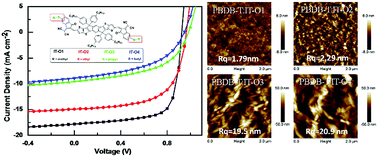
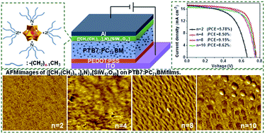
Youchun Chen, Simin Zhang, Qiming Peng, Lixin Wu, Fenghong Li, Yue Wang
The alkyl chain length of {[CH3(CH2)n-1]4N}4[SiW12O40] as a cathode interlayer can significantly affect the performance of polymer solar cells due to the different surface morphology of the films.
The content of this RSS Feed (c) The Royal Society of Chemistry
03 Jul 02:36
by Wei Chen, Fang-Zhou Liu, Xi-Yuan Feng, Aleksandra B. Djurišić, Wai Kin Chan, Zhu-Bing He
Abstract
Organic–inorganic hybrid perovskite solar cells have resulted in tremendous interest in developing next generation photovoltaics due to high record efficiency exceeding 22%. For inverted structure perovskite solar cells, the hole extraction layers play a significant role in achieving efficient and stable perovskite solar cell by modifying charge extraction, interfacial recombination losses, and band alignment. Here, cesium doped NiOx is selected as a hole extraction layer to study the impact of Cs dopant on the optoelectronic properties of NiOx and the photovoltaic performance. Cs doped NiOx films are prepared by a simple solution-based method. Both doped and undoped NiOx films are smooth and highly transparent, while the Cs doped NiOx exhibits better electron conductivity and higher work function. Therefore, Cs doping results in a significant improvement in the performance of NiOx-based inverted planar perovskite solar cells. The best efficiency of Cs doped NiOx devices is 19.35%, and those devices show high stability as well. The improved efficiency in devices with Cs:NiOx is attributed to a significant improvement in the hole extraction and better band alignment compared to undoped NiOx. This work reveals that Cs doped NiOx is very promising hole extraction material for high and stable inverted perovskite solar cells.

Cesium doping of NiOx enhances the conductivity of the oxide film and the hole extraction from the perovskite film in inverted planar perovskite solar cells. Significantly improved photovoltaic performance is obtained with the best efficiencies of 16.04% and 19.35% for NiOx and Cs:NiOx, respectively. The devices exhibit negligible hysteresis and good stability.
02 Jul 13:37
by Haonan Si, Qingliang Liao, Zhuo Kang, Yang Ou, JingJing Meng, Yichong Liu, Zheng Zhang, Yue Zhang
The NH4PbI3-based phase transformation is realized by simply adding NH4I additive, in order to simultaneously control perovskite nucleation and crystal growth. Regarding the nucleation process, the NH4+ with small ionic radius preferentially diffuses into the [PbI6]4− octahedral layer to form NH4PbI3, which compensates the lack of CH3NH3I (MAI) precipitation. The generation of NH4PbI3 intermediate phase results in extra heterogeneous nucleation sites and reduces the defects derived from the absence of MA+. Regarding the crystal growth process, the cation exchange process between MA+ and NH4+, instead of the MAs directly entering, successfully retards the crystal growth. Such NH4PbI3 consumption process slows down the crystal growth, which effectively improves the perovskite quality with lowered defect density. The cooperation of these two effects eventually leads to the high-quality perovskite with enlarged grain size, prolonged photoluminescence lifetime, lowered defect density, and increased carrier concentration, as well as the finally enhanced photovoltaic performance. Moreover, NH3 as a byproduct further facilitates the proposed transformation process and no external residue remains even without any post-treatment. Such methodology of introducing a novel phase transformation to simultaneously control nucleation and crystal growth processes is of universal significance for further devotion in the foreseeable perovskite solar cells (PSCs) evolution.

An innovative NH4I-induced phase transformation is designed to optimize the perovskite crystallization from both nucleation and crystal growth aspects. The rational designed intermediate phase NH4PbI3 simultaneously contributes to the extra heterogeneous nucleation sites and slows down crystal growth rate, which finally leads to the optimized perovskite quality and advanced photovoltaic performance with extra 10% improvement.
02 Jul 13:36
by Gurpreet S. Selopal, Haiguang Zhao, Xin Tong, Daniele Benetti, Fabiola Navarro-Pardo, Yufeng Zhou, David Barba, François Vidal, Zhiming M. Wang, Federico Rosei
Colloidal quantum dots (QDs) are widely studied due to their promising optoelectronic properties. This study explores the application of specially designed and synthesized “giant” core/shell CdSe/(CdS)x QDs with variable CdS shell thickness, while keeping the core size at 1.65 nm, as a highly efficient and stable light harvester for QD sensitized solar cells (QDSCs). The comparative study demonstrates that the photovoltaic performance of QDSCs can be significantly enhanced by optimizing the CdS shell thickness. The highest photoconversion efficiency (PCE) of 3.01% is obtained at optimum CdS shell thickness ≈1.96 nm. To further improve the PCE and fully highlight the effect of core/shell QDs interface engineering, a CdSexS1−x interfacial alloyed layer is introduced between CdSe core and CdS shell. The resulting alloyed CdSe/(CdSexS1−x)5/(CdS)1 core/shell QD-based QDSCs yield a maximum PCE of 6.86%, thanks to favorable stepwise electronic band alignment and improved electron transfer rate with the incorporation of CdSexS1−x interfacial layer with respect to CdSe/(CdS)6 core/shell. In addition, QDSCs based on “giant” core/CdS-shell or alloyed core/shell QDs exhibit excellent long-term stability with respect to bare CdSe-based QDSCs. The giant core/shell QDs interface engineering methodology offers a new path to improve PCE and the long-term stability of liquid junction QDSCs.

“Giant” alloyed CdSe/(CdSexS1−x)5/(CdS)1 core/shell quantum dots (QDs) show superior optoelectronic properties, such as broader absorption spectrum, and better carrier separation and transfer rate with respect to CdSe/(CdS)6 core/shell QDs. The alloyed core/shell QDs sensitized solar cells (QDSCs) exhibit a photoconversion efficiency of 6.86% and excellent long-term stability, and offer a new path for liquid junction QDSCs technology.
30 Jun 00:44
by Shuqiong Lan, Huihuang Yang, Guocheng Zhang, Xiaomin Wu, Qizhen Chen, Liang Chen, Huipeng Chen and Tailiang Guo

ACS Applied Materials & Interfaces
DOI: 10.1021/acsami.7b00781

30 Jun 00:41
by Jialin Wang, Jiajun Peng, Xiaoyu Liu and Ziqi Liang

ACS Applied Materials & Interfaces
DOI: 10.1021/acsami.7b03757

30 Jun 00:38
by Marcos A. Santana Andrade, Armi Tiihonen, Kati Miettunen, Peter Lund, Ana F. Nogueira and Heloise O. Pastore

ACS Applied Materials & Interfaces
DOI: 10.1021/acsami.7b00897

29 Jun 00:38
by Daqin Chen, Xiao Chen, Zhongyi Wan and Gaoliang Fang

ACS Applied Materials & Interfaces
DOI: 10.1021/acsami.7b05429

29 Jun 00:29
by Yafang Qi, Qingwen Tian, Yuena Meng, Dongxing Kou, Zhengji Zhou, Wenhui Zhou and Sixin Wu

ACS Applied Materials & Interfaces
DOI: 10.1021/acsami.7b03944

24 Jun 00:54
by Guifang Han, Teck Ming Koh, Swee Sien Lim, Teck Wee Goh, Xintong Guo, Shin Woei Leow, Raihana Begum, Tze Chien Sum, Nripan Mathews and Subodh Mhaisalkar

ACS Applied Materials & Interfaces
DOI: 10.1021/acsami.7b05133

24 Jun 00:35
by Hong-Hua Fang, Loredana Protesescu, Daniel M. Balazs, Sampson Adjokatse, Maksym V. Kovalenko, Maria Antonietta Loi
The optical properties of the newly developed near-infrared emitting formamidinium lead triiodide (FAPbI3) nanocrystals (NCs) and their polycrystalline thin film counterpart are comparatively investigated by means of steady-state and time-resolved photoluminescence. The excitonic emission is dominant in NC ensemble because of the localization of electron–hole pairs. A promisingly high quantum yield above 70%, and a large absorption cross-section (5.2 × 10⁻¹³ cm−2) are measured. At high pump fluence, biexcitonic recombination is observed, featuring a slow recombination lifetime of 0.4 ns. In polycrystalline thin films, the quantum efficiency is limited by nonradiative trap-assisted recombination that turns to bimolecular at high pump fluences. From the temperature-dependent photoluminescence (PL) spectra, a phase transition is clearly observed in both NC ensemble and polycrystalline thin film. It is interesting to note that NC ensemble shows PL temperature antiquenching, in contrast to the strong PL quenching displayed by polycrystalline thin films. This difference is explained in terms of thermal activation of trapped carriers at the nanocrystal's surface, as opposed to the exciton thermal dissociation and trap-mediated recombination, which occur in thin films at higher temperatures.

The newly developed formamidinium lead triiodide (FAPbI3) nanocrystals (NCs) show quantum yield above 70% with a large absorption cross-section (5.2 × 10⁻¹³ cm−2). Biexcitonic recombination is observed, featuring a slow recombination lifetime of 0.4 ns. The optical properties of the NC ensemble are further compared with their polycrystalline thin film counterpart, showing two very distinct recombination mechanisms.