ACS Applied Materials & Interfaces
DOI: 10.1021/acsami.7b11168
Organic-inorganic halide perovskite materials have become a shining star in the photovoltaic field due to their unique properties, such as high absorption coefficient, optimal bandgap, and high defect tolerance, which also lead to the breathtaking increase in power conversion efficiency from 3.8% to over 22% in just seven years. Although the highest efficiency was obtained from the TiO2 mesoporous structure, there are increasing studies focusing on the planar structure device due to its processibility for large-scale production. In particular, the planar p-i-n structure has attracted increasing attention on account of its tremendous advantages in, among other things, eliminating hysteresis alongside a competitive certified efficiency of over 20%. Crucial for the device performance enhancement has been the interface engineering for the past few years, especially for such planar p-i-n devices. The interface engineering aims to optimize device properties, such as charge transfer, defect passivation, band alignment, etc. Herein, recent progress on the interface engineering of planar p-i-n structure devices is reviewed. This review is mainly focused on the interface design between each layer in p-i-n structure devices, as well as grain boundaries, which are the interfaces between polycrystalline perovskite domains. Promising research directions are also suggested for further improvements.

Interface engineering has been widely practiced on planar p-i-n perovskite solar cells since it brings about significant improvement in both device performance and stability. Recent progress is reviewed about the engineering of each interface of such devices and its effects, including defect passivation, accelerated charge transfer, enhanced stabilities, etc., which are key parameters for the photovoltaic devices.
Charge extraction rate in solar cells made of blends of electron donating/accepting organic semiconductors is typically slow due to their low charge carrier mobility. This sets a limit on the active layer thickness and has hindered the industrialization of organic solar cells (OSCs). Herein, charge transport and recombination properties of an efficient polymer (NT812):fullerene blend are investigated. This system delivers power conversion efficiency of >9% even when the junction thickness is as large as 800 nm. Experimental results indicate that this material system exhibits exceptionally low bimolecular recombination constant, 800 times smaller than the diffusion-controlled electron and hole encounter rate. Comparing theoretical results based on a recently introduced modified Shockley model for fill factor, and experiments, clarifies that charge collection is nearly ideal in these solar cells even when the thickness is several hundreds of nanometer. This is the first realization of high-efficiency Shockley-type organic solar cells with junction thicknesses suitable for scaling up.

Strongly suppressed recombination is observed in a polymer:fullerene system resulting in solar cell power conversion efficiencies as high as 9% at a junction thickness of 800 nm. Results indicate that solar cell devices made of this material system with thicknesses as large as 300 nm can exhibit Shockley-type behavior, i.e., the fill factor is unaffected by bimolecular recombination.

In article number 1701164, Wallace C.H. Choy and co-workers demonstrate an all-solution-processed switchable interconnecting layer (ICL) for both inverted and normal tandem organic solar cells (OSCs). This strategy shifts the views from conventionally complicated tunneling junction ICL where both electron/hole transport layers play several different roles towards simplified ICL where electron/hole transport layers play distinct decoupled role, advancing ICL for more adaptable tandem OSCs.


Perovskite solar cells (PSCs) are one of the promising photovoltaic technologies for solar electricity generation. NiOx is an inorganic p-type semiconductor widely used to address the stability issue of PSCs. Although high efficiency is obtained for the devices employing NiOx as the hole transport layer, the fabrication methods have yet to be demonstrated for industrially relevant manufacturing of large-area and high-performance devices. Here, it is shown that these requirements can be satisfied by using the magnetron sputtering, which is well established in the industry. The limitations of low fill factor and short-circuit current commonly observed in sputtered NiOx-derived PSCs can be overcome through magnesium doping and low oxygen partial pressure deposition. The fabricated PSCs show a high power conversion efficiency of up to 18.5%, along with negligible hysteresis, improved ambient stability, and high reproducibility. In addition, good uniformity is also demonstrated over an area of 100 cm2. The simple and well-established approach constitutes a reliable and scale method paving the way for the commercialization of PSCs.

Industrially relevant manufacturing of perovskite solar cells is demonstrated with the magnetron sputtered NiMgOx, and the limitations of low fill factor and short-circuit current commonly observed in sputtered NiOx-derived devices can be overcome through magnesium doping and low oxygen partial pressure deposition. The as-fabricated devices show a high efficiency of up to 18.5%, along with good uniformity over a large-area of 100 cm2.
Two new planar small molecule acceptors (SMAs) with A2 = A1-D-A1 = A2 skeleton are designed and synthesized, where indacenodithiophene (IDT), benzothiadiazole (BT), and thiazolidine-2,4-dione (TD) are used as the central donor unit of D, the bridged group of A1 and the end group of A2, respectively. The final SMAs of BT2 and BT2b reveal high-lying the lowest unoccupied molecular orbital (LUMO) in comparison with that of rhodanine (R) based analogs, which can increase the open-circuit voltage (VOC) of P3HT-based solar cells. In addition, by modulating the side chains in the middle IDT unit, BT2b with octyl side chain has an obvious red-shifted absorption spectrum and stronger crystallinity than that of BT2 with 4-hexylphenyl side chain. Meanwhile, the different monomolecular packing of two SMAs can be further proven from STM images, where only BT2b can form a regular texture. P3HT:BT2 and P3HT:BT2b blend solar cells upon thermal annealing shows power conversion efficiencies (PCEs) of 4.93 and 6.08% with open-circuit voltage (VOC) of 0.97 and 0.92 V, respectively. The results indicate that TD is a promising end-caped segment to up-shift the LUMO of BT-based SMAs and could simultaneously realize high VOC and PCE. In addition, the different side chains attached in IDT unit can strongly affect the intermolecular interaction and photovoltaic performance. These results provide important guideline for the design of SMAs to combine with P3HT.

Benzothiadiazole (BT) is a kind of important electron-accepting building block to construct photovoltaic materials. As electron acceptor to combine with classic P3HT donor, BT-based polymer acceptors exhibit high VOC but low PCE, and double-BT based small molecules realize high PCE but low VOC. Here, thiazolidine-2,4-dione is introduced to synthesize BT2 and BT2b with high LUMO energy levels. The P3HT:BT2b based solar cell could simutanously achieve a high VOC of 0.92 V and a promising PCE of 6.08%.
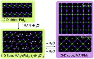
In spite of perovskite solar cells have achieved great progress in recent years, the long term stability of perovskite material is always a big obstacle before commercialization, especially the moisture instability. In this paper, we reported a layered perovskite solar cell based on (CF3CH2NH2)2(FA0.825MA0.15Cs0.025)n−1Pbn(I0.85Br0.15)3n+1 series (n = 1−∞), which possess excellent optoelectronic property and stability. The perovskite film displayed an ultrahigh surface coverage and provided high-quality thin films which lead to an advancement in solar cells performance. We had fabricated solar cells based on (CF3CH2NH2)2(FA0.825MA0.15Cs0.025)29Pb30(I0.85Br0.15)91 light absorber and got the best PCE of 18.17%. The average PCE of 17.84% was achieved with Jsc of 21.05 mA cm−2, Voc of 1.095V, and FF of 77.4%. Moreover, the multi-layered perovskite showed excellent property of moisture-resistant compared to three-dimensional type PSCs. Under relative humidity level of 65%, the devices without any encapsulation did not deteriorate for up to approximately 28 days with the PCE maintaining over 90%.

A mixed-dimensionality and mixed-compositional (MDMC) perovskite based on [CF3CH2NH2]2(FA0.825MA0.15Cs0.025)n−1Pbn(I0.85Br0.15)3n+1 series (n = 1−∞) is reported. The perovskite film was easy to yield high-quality films, and an overall power conversion efficiency over 18% was achieved in this perovskite system. Moreover, the perovskite solar cells based on this multilayered structures show the capacity of excellent resistance to moisture.
Recently, perovskite/Si devices have attracted enormous interest as an ideal technology for tandem cells, particularly due to the attributes from perovskite cell including low temperature processibility, tunable optical bandgap, and high open circuit voltage. Although solution process is considered to be cost effective and more widely adoptable for perovskite subcell, to the best of our knowledge, there has been no successful demonstration for the resulting high performance two-terminal perovskite/Si cells. In this manuscript, solution process is employed to fabricate the key components in the two-terminal perovskite/Si tandem solar cell, including tunneling junction and the perovskite absorber. The current density match between both cells is thoroughly studied by varing the perovskite bandgap from ≈1.55 to 1.69 eV. It was also revealed that the photovoltage modulation in the device is primarily associated to the band alignment over the perovskite and the tunneling materials. Therefore, a reverse scanned power conversion efficiency over 20% is demonstrated, the most efficient two-terminal perovskite/Si device based on solution processed perovskite subcells.

A solution process is employed to fabricate two-terminal perovkite/Si tandem solar cell with power conversion efficiency over 20%, where the photocurrent match and the photovoltage loss in the tandem cell is thoroughly studied.
Graphene-on-semiconductor has been proved to be a quality heterojunction with efficient photoelectric conversion. Graphene serves multiple functions as transparent electrode, active junction layer, hole collector, and anti-reflection layer in heterojunction photodevices, such as solar cells and photodetectors, and could be extended to other optoelectronics. Antimony sulfide (Sb2S3), a promising and readily available absorber material, is widely employed in low-cost and environmentally friendly solar cells. However, current Sb2S3 thin-film solar cells mostly use organic material as the hole-transporting layer and suffer from unsatisfactory stability. Here, graphene is selected as a hole-transporting layer to construct novel planar graphene/Sb2S3 based full-inorganic thin film solar cell and visible-light photodetector. By modifying the surface of Sb2S3 to reduce surface defects and balancing the transparency and conductivity of graphene layers, the solar cell records an overall power conversion efficiency of 1.65%, as well as an open circuit voltage of 0.665 V under AM 1.5G illumination (100 mW cm−2). The device shows almost no degradation even after 2 months of ambient storage. Moreover, the device with high a built-in electric field as photoanode is applied to detect the visible light without a power source. This self-powered light-photodetector exhibits good visible-light response, linear photocurrent characteristics, high stability, excellent reproducible properties, and fast photoresponse. These findings are believed to consequently spur further attempts to bridge graphene and semiconductor towards the promising goal of harvesting solar energy.

Graphene is transferred on the surface of Sb2S3 to serve as a promising ultrathin nanoscale hole-selective layer, enabling efficient fully inorganic thin film solar cell and self-powered visible light photodetector. This study provides a new concept for the design of Sb2S3 thin film optoelectronic device with long-term stability, processing easiness, and potential scalability over large areas.
Metallic nanoparticles (NPs) exhibit a surface plasmon resonance (SPR) and can be incorporated into perovskite solar cells (PSCs) to improve cell performance. However, the incorporation of Au NPs in bulk films of PSCs requires large concentration to keep interval distance and would cause worse device performance. In this work, a universal strategy for significant increasing power conversion efficiency (PCE) of PSCs through incorporating high aspect ratio Au nanorods (NRs)@SiO2 into perovskite/spiro-OMeTAD interface is demonstrated. The key feature of this approach is that we can take advantage of the SPR at a lower concentration and the Au NRs have larger light scattering section than AuNPs. It is found that the SPR and scattering effect of Au NRs lead to a broad enhancement of photon absorption. Furthermore, a superior enhanced charge separation process in the Au NRs incorporated device is also observed. Benefitting from this cooperative plasmonic effect of Au NRs in optical and electrical aspects, both short-circuit current density and open-circuit voltage are improved, resulting in the new device delivering a PCE up to 17.39% from 14.39%. This result further supports that Au NRs can play a more effective SPR effect at perovskite/spiro-OMeTAD interface, rather than incorporating them into bulk films.

A universal strategy for a significant increase in power conversion efficiency of perovskite solar cells through the incorporation of high aspect ratio Au nanorods@SiO2 into perovskite/spiro-OMeTAD interface is demonstrated. The plasmonic and scattering effects of Au NRs lead to a broad enhancement of photon absorption and a superior improvement of charge separation. This cooperative plasmonic effect in optical and electrical aspects finally delivers the cell efficiency up to 17.39% from 14.39%.
The influence of ZnO seed layer thickness in Squaraine (SQ) is investigated: PC71BM bulk heterojunction solar cells that incorporate ZnO nanorods. The thickness of the ZnO seed layer varies between 16–249 nm by changing the concentration of the precursor solution. With atomic force microscopy (AFM), X-Ray Diffraction (XRD), and Scanning Electron Microscopy (SEM) studies, it is shown that this approach allows to systematically tune the thickness of the ZnO seed layer without influencing seed layer grain size, or the morphology of the ZnO nanorods that are deposited on top of the seed layer. The proof-of-concept is demonstrated in SQ:PC71BM solar cells. It is found that seed layers with 55 nm thickness yield the highest short circuit current densities, resulting in power conversion efficiencies of 2.5 ± 0.1%. These results are compared to SQ:PC71BM solar cells prepared in planar architectures, and it is observed that both device architectures yield comparable results. The optimized nanostructured ZnO electrode enables the fabrication of BHJ devices with thick active layers without the loss in solar cell performance.

An approach to fabricate Squaraine (SQ):PC71BM bulk heterojunction solar cells with thick active layers is demonstrated. ZnO nanorods are used as the electron transport layer, and the active layer is infiltrated into the nanoarray. Varying the thickness of the ZnO seed layer does not influence the morphology of the nanorods, allowing to optimize the electron transport layer in the solar cell.

A novel patterning method for perovskite thin films is developed by Dae-Hyeong Kim and co-workers, which is described in article number 1702902. The patterning method (spin-on-patterning) is based on the thermodynamically preferred dewetting behavior of the perovskite precursor solution during the spin-coating process. By using this method, a high-performance, ultrathin, and deformable perovskite-on-silicon multiplexed image sensor array is successfully achieved.
Improving the fill factor (FF) is known as a challenging issue in organic solar cells (OSCs). Herein, a strategy of extending the conjugated area of end-group is proposed for the molecular design of acceptor–donor–acceptor (A–D–A)-type small molecule acceptor (SMA), and an indaceno[1,2-b:5,6-b′]dithiophene-based SMA, namely IDTN, by end-capping with the naphthyl fused 2-(3-oxocyclopentylidene)malononitrile is synthesized. Benefiting from the π-conjugation extension by fusing two phenyls, IDTN shows stronger molecular aggregation, more ordered packing structure, thus over one order of magnitude higher electron mobility relative to its counterpart. By utilizing the fluorinated polymer (PBDB-TF) as the electron donor, the corresponding device exhibits a high efficiency of 12.2% with a record-high FF of 0.78, which is approaching the theoretical limit of OSCs. Compared with the reference molecule, such a high FF in the IDTN system can be mainly attributed to the more ordered π–π packing of acceptor aggregates, higher domain purity and symmetric carrier transport in the blend. Hence, enlarging the conjugated area of the terminal-group in these A–D–A-type SMAs is a promising approach not only for enhancing the electron mobility, but also for improving the blend morphology, and both of them are conducive to the fill-factor breakthrough.

By extending the conjugated area of the end-group, a newly designed A–D–A–type small-molecule acceptor, namely IDTN, exhibits dense and ordered packing, and therefore, the electron mobility of the IDTN is over one order of magnitude higher than that of its counterpart. When blended with the donor polymer PBDB-TF, a high efficiency of 12.2% with an outstanding fill factor of 0.78 is achieved.
Low temperature solution processed planar-structure perovskite solar cells gain great attention recently, while their power conversions are still lower than that of high temperature mesoporous counterpart. Previous reports are mainly focused on perovskite morphology control and interface engineering to improve performance. Here, this study systematically investigates the effect of precise stoichiometry, especially the PbI2 contents on device performance including efficiency, hysteresis and stability. This study finds that a moderate residual of PbI2 can deliver stable and high efficiency of solar cells without hysteresis, while too much residual PbI2 will lead to serious hysteresis and poor transit stability. Solar cells with the efficiencies of 21.6% in small size (0.0737 cm2) and 20.1% in large size (1 cm2) with moderate residual PbI2 in perovskite layer are obtained. The certificated efficiency for small size shows the efficiency of 20.9%, which is the highest efficiency ever recorded in planar-structure perovskite solar cells, showing the planar-structure perovskite solar cells are very promising.

Planar-structure perovskite solar cells with efficiencies of 21.6% in small size (0.0737 cm2) and 20.1% in large size (1 cm2) with moderate residual PbI2 in perovskite layer are obtained. The certificated efficiency for small size shows the efficiency of 20.9%, which is the highest efficiency ever recorded in planar-structure perovskite solar cells.
Compact TiO2 is widely used as an electron transport material in planar-perovskite solar cells. However, TiO2-based planar-perovskite solar cells exhibit low efficiencies due to intrinsic problems such as the unsuitable conduction band energy and low electron extraction ability of TiO2. Herein, the planar TiO2 electron transport layer (ETL) of perovskite solar cells is modified with ionic salt CuI via a simple one-step spin-coating process. The p-type nature of the CuI islands on the TiO2 surface leads to modification of the TiO2 band alignment, resulting in barrier-free contacts and increased open-circuit voltage. It is found that the polarity of the CuI-modified TiO2 surface can pull electrons to the interface between the perovskite and the TiO2, which improves electron extraction and reduces nonradiative recombination. The CuI solution concentration is varied to control the electron extraction of the modified TiO2 ETL, and the optimized device shows a high efficiency of 19.0%. In addition, the optimized device shows negligible hysteresis, which is believed to be due to the removal of trap sites and effective electron extraction by CuI-modified TiO2. These results demonstrate the hitherto unknown effect of p-type ionic salts on electron transport material.

It is revealed that the CuI islands on the TiO2 electron transport layer can induce change of polarity increasing electron extraction, establish barrier-free band alignment with perovskite, and reduce the trap sites. These changes of interface properties induce power conversion efficiency of 19.0% perovskite solar cell with negligible hysteresis.

Organic-inorganic mixed perovskite solar cells demonstrate superiority for the application as low-cost printable solar energy, yet common processing of solvent-controlled crystallization routes contain highly toxic solvents that cause safety and/or environmental issues. In article number 1700576, Fuzhi Huang, Jie Zhong, and co-workers demonstrate a green solvent engineering incorporated interface optimization method to address this topic, and high performance devices are obtained.

In article number 1700977, Yana Vaynzof and co-workers investigate how the MAPbI3 perovskite layer microstructure is affecting its stability upon exposure to oxygen and light. The authors show that the degradation process is initiated at the grain boundaries, demonstrating that devices whose active layer consists of larger, more uniform grains exhibit enhanced photovoltaic stability.

In article number 1700265, Annalisa Bruno and co-workers show that applying an electrical poling to precondition the SCs below 170 K, the MA+ cations can be efficiently oriented and I− accumulation at the TiO2/MAPbI3 interface is facilitated. Both phenomena lead to improved charge transfer efficiency at the interface. In the cover, the MAPbI3 and TiO2 interface in a solar cell at low temperature under electrical poling is highlighted.
Herein, this study reports high-efficiency, low-temperature ZnO based planar perovskite solar cells (PSCs) with state-of-the-art performance. They are achieved via a strategy that combines dual-functional self-assembled monolayer (SAM) modification of ZnO electron accepting layers (EALs) with sequential deposition of perovskite active layers. The SAMs, constructed from newly synthesized molecules with high dipole moments, act both as excellent surface wetting control layers and as electric dipole layers for ZnO-EALs. The insertion of SAMs improves the quality of PbI2 layers and final perovskite layers during sequential deposition, while charge extraction is enhanced via electric dipole effects. Leveraged by SAM modification, our low-temperature ZnO based PSCs achieve an unprecedentedly high power conversion efficiency of 18.82% with a VOC of 1.13 V, a JSC of 21.72 mA cm−2, and a FF of 0.76. The strategy used in this study can be further developed to produce additional performance enhancements or fabrication temperature reductions.

Low-temperature planar perovskite solar cells with efficiency of 18.82% are developed via a strategy that combines dual-functional self-assembled monolayer (SAM) modification of ZnO electron accepting layers with sequential deposition of perovskite active layers. The SAMs, constructed from newly synthesized molecules with high dipole moments, act both as excellent surface wetting control layers and as electric dipole layers for ZnO layers.