09 Jun 00:58
by Tingting Yan,
Ziqing Li,
Fa Cao,
Jiaxin Chen,
Limin Wu,
Xiaosheng Fang

An all-organic self-powered photodetector with ultraflexibility and dual-polarity output is successfully fabricated by an all-solution method, which is expected to have great application potential in realizing multifunctional, portable, and wearable electronic devices.
Abstract
Endowing photodetectors with mechanically flexibility and actual functionality are current research issues in developing optoelectronic devices. However, rigid metal-based or metal-oxide-based electrodes remain a block to the realization of ultraflexible electronics. Thus, an ultraflexible all-organic photodetector (all-OPD) is designed by innovatively introducing symmetrical organic electrodes PH1000/PH1000 to substitute the widely applied indium-doped tin oxide (ITO)/Ag electrodes. Specifically, this all-OPD exhibits a high self-powered responsivity (R) of over 100 mA W−1 among 500–600 nm and the photocurrent remains about 80% of the original performance after being bent 20 000 circles, and can output steady biosignals for photo-plethysmography (PPG) application. More importantly, this all-OPD outputs dual-polarity photocurrent as it is flipped or folded. Benefitting from the ordered phase distribution and designed Schottky barrier heights, the photogenerated holes will be transferred and collected by nearer electrode, while electrons will be trapped in the thick bulk heterojunction (BHJ) as a result of the long channel. This work offers a new avenue toward developing a multifunctional and ultraflexible all-OPD with a straightforward all-solution method, and it is expected to be more compatible in complex application scenarios.
14 Apr 01:38
by Yuyan Zhao,
Jiangang Feng,
Gaosong Chen,
Jun‐Jie Wu,
Xue‐dong Wang,
Lei Jiang,
Yuchen Wu

Deterministic patterning of colloidal quantum dots into high-quality micro-/nanostructures is developed for the construction of multifunctional integrated photonic devices. Mode-tunable microlasers and waveguides are coupled to direct on-chip generation and propagation of coherent light, which permits a proof-of-concept demonstration of integrated photonic circuits for encoding photonic outputs into information bits.
Abstract
Colloidal quantum dots (CQDs) are promising for photonic applications toward lasers, waveguides, and photodetectors. However, integration of high-quality photonic elements into multifunctional devices is still restricted by optical losses stemming from the accumulation of defects and disorder in the solution process. Herein, a platform with a directional Laplace pressure is created for eliminating undesired pinning of liquid fronts in the solution process and boosting ordered assembly of CQDs into designable micro-/nanostructures. The versatility and robustness of this method are demonstrated by deterministic patterning of CQDs with different components and photoluminescence spectra onto various substrates. On the basis of this platform, microring lasers with tunable emission modes, low-loss waveguides, and their coupled structures have been reached for direct on-chip generation and propagation of coherent light. A proof-of-concept demonstration of integrated circuits is also conducted by combining microcavity lasers with waveguides for encoding photonic outputs into information bits.
14 Apr 00:58
by Kumar Mallem, Maksym F. Prodanov, Chen Dezhang, Mikita Marus, Chengbin Kang, Sunil B. Shivarudraiah, Valeri V. Vashchenko, Jonathan E. Halpert, and Abhishek K. Srivastava

ACS Applied Materials & Interfaces
DOI: 10.1021/acsami.2c04466
28 Mar 03:09
by Namkyu Lee,
Joon‐Soo Lim,
Injoong Chang,
Hyung Mo Bae,
Juyeong Nam,
Hyung Hee Cho

Flexible assembled metamaterials (FAM) overcome the material flexibility as well as unit cell size disparities to operate the infrared and microwave camouflage simultaneously in a single material. The authors evaluate the contrast radiant intensity (CRI, infrared) and radar cross section (RCS, microwave) to illustrate FAM's infrared and microwave camouflage capability on the application.
Abstract
Light, heat, and waves in electromagnetic energy are the foundation for the advancement of human being. Camouflage materials based on metamaterials are used to excel the performance limits by manipulating the electromagnetic energy. However, multispectral camouflage materials with flexibility are difficult to fabricate because required radiative properties in each spectral regime are different and have largely different scales of the unit cell in a single structure. The authors propose flexible assembled metamaterials (FAM) by assembling the flexible infrared (IR) emitter and flexible microwave absorber. The authors adopt the intermediate layer to assemble the IR emitter and the microwave absorber, leading to securing the selective emission in IR wave measured by Fourier-transform infrared spectroscopy (FT-IR) measurement and broadening the wavelength of microwave absorption. They calculate the energy dissipation of accumulated energy due to the lowering the radiative energy in the IR regime similar to that of conventional camouflage materials. The wavelength having required absorption (>0.9) for microwave camouflage is wider 2–12 GHz than the conventional microwave absorber. FAM demonstrate multispectral camouflage performances through the decrease in the contrast radiant intensity for IR wave by 75% and the radar cross section for microwave by 99% compared to reference surfaces.
18 Mar 02:48
by Soumyadipta Rakshit,
Piotr Piatkowski,
Iván Mora‐Seró,
Abderrazzak Douhal

Strategies for improving the performance of perovskite-based solar cells, light emitting diodes, and photodetectors by integrating different quantum dots through the enhancement of interface controlled nucleation, stability, and charge transport of perovskite layer are critically analyzed and summarized.
Abstract
Metal halide perovskites having high defect tolerance, high absorption characteristics, and high carrier mobility demonstrate great promise as potential light harvesters in photovoltaics and optoelectronics and have experienced an unprecedented development since their occurrence in 2009. Semiconductor quantum dots (QDs), on the other hand, have also been proved to be very flexible toward shape, dimension, bandgap, and optical properties for constructing optoelectronic devices. Of late, a strategic combination of both materials has demonstrated extraordinary promise in photovoltaic applications and optoelectronic devices. Combining QDs and perovskites has proved to be quite an effective strategy toward the formation of pinhole-free and more stable perovskite crystals along with tunability of other properties. To boost this exciting research field, it is imperative to summarize the work done so far in recent years to provide an intriguing insight. This review is a critical account of the advanced strategy toward combining these two fascinating materials, including their different synthetic approaches regarding heteroepitaxial growth of perovskite crystals on QDs, carrier dynamics at the interface and potential application in the field of solar cells, light emitting diodes, and photodetectors.
18 Mar 02:48
by Jiangyong Pan,
Zihan Zhao,
Fan Fang,
Lixi Wang,
Guangzhao Wang,
Chengjun Liu,
Qianqian Huang,
Jinyi Sun,
Yuling Huang,
Lei Mao,
Jing Xie,
Ying Xue,
Jing Chen,
Wei Lei

A strategy of codoping Mn2+ and Ni2+ in CsPb(Br/Cl)3 is developed to improve the photoluminescence quantum yield and thermal stability of perovskite quantum dots (PeQDs) due to the defect passivation and enhanced formation energy. The resulting PeQD light-emitting diodes exhibit the maximum external quantum efficiency of 3.31% with the emission peak located at 469 nm, and lifetime exceeding 8 min.
Abstract
Highly efficient green and red perovskite quantum dots (PeQDs) light-emitting diodes (PeQDLEDs) have been achieved. However, blue PeQDLEDs, especially those with the relatively short wavelengths (<470 nm) meeting National Television System Committee blue standard, have struggled to match the high efficiency and stability of their red and green counterparts. The main critical problems are the low photoluminescence quantum yield (PLQY) and poor stability of PeQDs, as well as the unfavorable device structure. Herein, a strategy of codoping Mn2+ and Ni2+ in CsPb(Br1.8Cl1.2) is developed to improve the PLQY and thermal stability of PeQDs due to the defect passivation and enhanced formation energy. Meanwhile, the valence band position of PeQDs is elevated to reduce the hole injection barrier benefitting from the synergetic codoping strategy. As a result, the PeQDLEDs based on codoped PeQDs exhibit the maximum external quantum efficiency (EQE) of 3.31% with the emission peak located at 469 nm, and lifetime exceeding 8 min. The work provides a new avenue to achieve efficient and stable pure blue PeQDLEDs.
18 Mar 02:44
by Zhourui Xu, Zhijun Zhang, Xiangquan Deng, Jiangao Li, Yihang Jiang, Wing-Cheung Law, Chengbin Yang, Wanjian Zhang, Xiaolin Chen, Ke Wang, Dong Wang, and Gaixia Xu

ACS Nano
DOI: 10.1021/acsnano.2c01349
18 Mar 02:36
by Oleg P. Dimitriev

Chemical Reviews
DOI: 10.1021/acs.chemrev.1c00648
18 Mar 02:36
by Shuai Yuan, Xiaopeng Zheng, Wan-Shan Shen, Jiakai Liu, Lin-Song Cui, Congcong Zhang, Qi-Sheng Tian, Jun-Jie Wu, Yu-Hang Zhou, Xue-Dong Wang, Zhao-Kui Wang, Peigang Han, Joseph M. Luther, Osman M. Bakr, and Liang-Sheng Liao

ACS Energy Letters
DOI: 10.1021/acsenergylett.2c00465
18 Mar 02:03
by Yingjie Chai, Xiaobo Zhou, Xinyu Chen, Chenqing Wen, Jiaming Ke, Wei Feng, and Fuyou Li

ACS Applied Materials & Interfaces
DOI: 10.1021/acsami.1c21838
18 Mar 01:55
by Guannan Zhang, Hanyuan Zhang, Rui Yu, Yongqing Duan, YongAn Huang, and Zhouping Yin

ACS Applied Materials & Interfaces
DOI: 10.1021/acsami.1c23630
18 Mar 01:54
Nanoscale, 2022, 14,4123-4130
DOI: 10.1039/D1NR07007J, Paper
Matthias Ruppert, Hanh Bui, Laxmi Kishore Sagar, Pieter Geiregat, Zeger Hens, Gabriel Bester, Nils Huse
Femtosecond pump–probe spectroscopy reveals ultrafast carrier dynamics in mid-infrared (MIR) colloidal HgTe nanoparticles with a bandgap of 2.5 μm at a mean energy dissipation rate of 0.36 eV ps−1 irrespective of excitation wavelength.
The content of this RSS Feed (c) The Royal Society of Chemistry
07 Mar 01:23
by Luyao Mei,
Runfeng Huang,
Chaorong Shen,
Jianguo Hu,
Pu Wang,
Zhengji Xu,
Zhanfeng Huang,
Lu Zhu

Near-infrared photodetectors and imaging arrays employing hybrid Pb-/Sn-/SnPb-based perovskites are reviewed comprehensively. The latest progress of these near-infrared devices is discussed in terms of perovskite formation, device structures, working mechanisms, and device performances. Potentials including spectral response extension, pixel integration, flexible devices, and stability are introduced to advance perovskite-based near-infrared devices toward commercialization.
Abstract
Hybrid halide perovskites have been demonstrated to be prospective materials in optoelectronic devices due to their outstanding photoelectric properties and facile manufacturability by low-cost and fast solution-processed methods. Particularly, to meet increasingly potential applications in near-infrared (NIR) detection and imaging, perovskites have been introduced and explored their roles, some of which achieve the comparable performance with traditional silicon counterparts. Here, the recent advancements of hybrid halide perovskite-based NIR photodetectors and imaging arrays in terms of perovskite formation, device structures, working mechanisms, and device performances are reviewed. Pb perovskite-based devices either employ sub-bandgap absorption and intraband transition, or incorporate with narrow-bandgap semiconductors to achieve NIR detection, which could reach the spectral response onset at 2.6 µm wavelength. Sn perovskite-based devices employ the strategies of template-assisted engineering and reducing additives to inhibit the oxidation of Sn2+ states for efficient detection. SnPb mixed perovskite devices employ compositional engineering, passivation strategies, crystallization tuning, and encapsulation to achieve efficient and long shelf-life photodetectors with an external quantum efficiency of 70% at 940 nm wavelength. Finally, potential prospects are proposed, including spectral response extension, pixel integration, flexible devices, and stability, to advance perovskite-based NIR detection and imaging toward commercial applications.
07 Mar 01:23
Nanoscale, 2022, 14,4263-4270
DOI: 10.1039/D2NR00544A, Paper
Kunlun Liu, Jun Zhao, Gencai Pan, Yaxian Zhu, Wenwu You, Huafang Zhang, Huiping Gao, Yanli Mao
CsPbI3 PQDs have been encapsulated in porous CaF2:Ce,Tb nanoarchitectures, which not only improved the stability of PQDs, but also maintained the high photoluminescence quantum yield (PLQY) of PQDs, benefitting from the sensitization of Tb3+ ions.
The content of this RSS Feed (c) The Royal Society of Chemistry
07 Mar 01:20
by Ahmad R. Kirmani, Michael Woodhouse, and Joseph M. Luther

ACS Energy Letters
DOI: 10.1021/acsenergylett.2c00250
07 Mar 01:19
by Maninderjeet Singh, Aman Agrawal, Wenjie Wu, Ali Masud, Edward Armijo, Damian Gonzalez, Shenghui Zhou, Tanguy Terlier, Chenhui Zhu, Joseph Strzalka, Krzysztof Matyjaszewski, Michael Bockstaller, Jack F. Douglas, and Alamgir Karim

ACS Applied Materials & Interfaces
DOI: 10.1021/acsami.1c23865
07 Mar 01:16
by Zong‐Liang Tseng,
Lung‐Chien Chen,
Li‐Wei Chao,
Meng‐Ju Tasi,
Dian Luo,
Nurul Ridho Al Amin,
Shun‐Wei Liu,
Ken‐Tseng Wong

A comprehensive optimization strategy, including 2-phenylethylammonium ligand (PEA+)-passivated FAPbI3 quantum dots (QDs), synergistic coverage effects between the QDs and hole-transporting layers, and effective electron-transporting layers for constructing a feasible device structure leads to a high-efficiency near-infrared (NIR) QD-based light-emitting diode (QLED) centered at 772 nm and exhibiting a maximum external quantum efficiency up to 15.4%, the highest external quantum efficiency recorded for perovskite-based NIR QLEDs.
Abstract
In recent years, the performance of perovskite quantum dots (QDs) and QD-based light-emitting diodes (QLEDs) has improved greatly, with electroluminescence (EL) efficiency of green and red emission exceeding 20%. However, the development of perovskite near-infrared (NIR) QLEDs has reached stagnation, where the reported maximum EL efficiency is still below 6%, limiting their further applications. In this work, new NIR-emissive FAPbI3 QDs are developed by post-treating long alkyl-encapsulated QDs with 2-phenylethylammonium iodide (PEAI). The incorporation of PEAI reduces the QD surface defects for giving a high photoluminescence quantum yield up to 61.6%. The n-octane solution of PEAI-passivated FAPbI3 QDs is spin coated on top of the PEDOT:PSS-treated ITO electrode modified with a thermally crosslinked hole-transporting layer to give a full-coverage, smooth, and dense QD film. Incorporating with an effective electron-transporting material, CN-T2T, which has deep lowest unoccupied molecular orbital and good electron mobility, the optimal device with EL λmax at 772 nm achieves an external quantum efficiency up to 15.4% at a current density of 0.54 mA cm−2 (2.6 V), which is the highest efficiency ever reported for perovskite-based NIR QLEDs. This study provides a facile strategy to prepare high-quality perovskite QD films suitable for highly efficient NIR QLED applications.
07 Mar 01:16
by Mokurala Krishnaiah,
Seungyeob Kim,
Ajit Kumar,
Dhananjay Mishra,
Seung Gi Seo,
Sung Hun Jin

Air-stable Cs2SnI6 (CSI) particles via hydriodic acid precursor optimization are reported. For system-level demonstration, physically detachable 3 × 3 photodector (PD) arrays, assembled with micro-light-emitting-diodes (µ-LEDs) as light sources, are demonstrated to cover the broadband spectrum of UV–visible–near-Infrared (NIR) and hold great promise for future wireless optical interconnection.
Abstract
With the surge in perovskite research, practical features for future applications are desired to be secured, but the reliability of the materials and the use of hazardous Pb are longstanding problems. Here, an air-stable Cs2SnI6 (CSI) is prepared via diluted hydriodic acid solvent-based precursor optimization during scalable hydrothermal growth. Materials characterization is performed using various elemental peak analyses and crystallographic identification. The resulting CSI exhibits long-term operating stability over 6 months, i) at elevated temperatures, ii) in ambient air, and iii) under light illumination from UV to near-infrared. More importantly, to demonstrate an intriguing class of applications up to system level, physically detachable CSI photodetector arrays (PD-arrays), integrated with micro-light-emitting-diodes (μ-LEDs) arrays, are successfully fabricated. In addition, 3 × 3 flexible CSI PDs are fully operational, even in air, and their spatial uniformity in pixels is quantitatively evaluated. The charge-transport mechanisms of the CSI PDs under light and elevated temperature are assessed via temperature-dependent characterization from 148 to 373 K, implying the involvement of 3D variable-range hopping. Multicycle evaluation of the CSI PD-arrays confirms their operational stability in AC and DC modes, demonstrating this platform's potential benefit for wireless optical interconnection in advanced Si technology.
07 Mar 01:15
Publication date: 1 June 2022
Source: Solar Energy Materials and Solar Cells, Volume 239
Author(s): Ankita Kolay, Debanjan Maity, Heather Flint, Elizabeth A. Gibson, Melepurath Deepa
07 Mar 00:42
by Yoshimi Inaba
Scientific Reports, Published online: 04 March 2022; doi:10.1038/s41598-022-07525-5
Spontaneous patterning method utilizing transformation of UV-curable emulsion
07 Mar 00:41
by Weijian Wang, Gang Yu, Sanam Attique, Weizhen Ye

The effect of charge transport material on the overall optical performance of the device is examined by finite element method. Density functional theory calculates the microstructure of the charge transport layer material and comprehends the energy level matching of the device. Combining micro- and macroscales facilitates the development of high-efficiency perovskite solar cells.
CsPbBr3 film possesses high stability and easy manufacturing characteristics, rendering it attractive for applications in perovskite solar cells (PSCs). However, optical loss and energy level matching of different material layers are still the major factors, limiting the performance of PSCs. Herein, the finite element method (FEM) and density functional theory (DFT) calculations composed of simulation interaction technology are used to study the effects of different electron transport layer and hole transport layer materials on the optical performance of different PSC configurations. The effect of the charge transport layer (CTL) material and CsPbBr3 on the energy level matching and charge transport of the device is explained. The FEM simulation results show that inorganic CTL materials produce less parasitic absorption than the organic materials. The DFT calculation results give the microscopic design rules of the CTL material. In addition, PSCs with a light-trapping structure are designed, which effectively suppressed surface reflection. Finally, through the screening of CTL materials and the design of advanced light-trapping structures, the photocurrent of PSCs is increased by 69.8% (from 5.30 to 9.00 mA cm−2). This work provides a novel model for the screening of CTL materials for inorganic PSCs.
27 Feb 13:19
by Ruiheng Chang, Kexin Wang, Youwei Zhang, Tianzi Ma, Jianwei Tang, Xue-Wen Chen, Butian Zhang, and Shun Wang

ACS Applied Materials & Interfaces
DOI: 10.1021/acsami.1c10888
27 Feb 13:19
by Jie Qiao,
Fu Feng,
Shuang Song,
Tao Wang,
Mengyan Shen,
Guoping Zhang,
Xiaocong Yuan,
Michael G. Somekh

Near-infrared photodetectors based on a CH3NH3PbI3 quantum dots (MQDs)/Ta2NiSe5 mixed-dimensional van der Waals heterostructure (MvdWHs) with a responsivity of 2.4 × 10² A W−1 and a detectivity of 6.0 × 10² Jones is reported, indicating that the optoelectrical properties of two-dimensional ternary Ta2NiSe5 can be significantly optimized via hybridization with MQDs and will accelerate the evolution of MvdWHs-based devices.
Abstract
2D materials and their van der Waals heterostructures are of great fundamental interest and have potential applications in emerging electronics devices. However, atomically thin photodetector applications have suffered from performance limitations because of low optical absorption. Here, a near-infrared photodetector based on methylammonium lead halide perovskite quantum dots (MQDs), combined with Ta2NiSe5 van der Waals heterostructures, is fabricated to take advantage of their energy band alignment. An ultrasensitive photoresponse with a detectivity of 6.0 × 10¹² Jones for 800 nm illumination is demonstrated. Furthermore, the field-effect mobility and responsivity are enhanced by factors of 2 and 7.4, respectively, by interfacing Ta2NiSe5 and the MQDs. These results indicate that the optoelectrical properties of 2D ternary Ta2NiSe5 can be significantly optimized via hybridization with MQDs and can accelerate the evolution of MQD-van der Waals heterostructure-based devices.
27 Feb 13:19
by Changting Wei,
Wenming Su,
Jiantong Li,
Bo Xu,
Qinsong Shan,
Ye Wu,
Fengjuan Zhang,
Manman Luo,
Hengyang Xiang,
Zheng Cui,
Haibo Zeng

An environmentally-friendly ternary-solvent-ink system with excellent printability and film-forming ability is tailor-made for efficient inkjet-printed perovskite quantum dot light-emitting diodes (QLEDs). A record peak external quantum efficiency (EQE) of 8.54% is achieved in inkjet-printed green perovskite QLEDs for the first time.
Abstract
Toward next-generation electroluminescent quantum dot (QD) displays, inkjet printing technique has been convinced as one of the most promising low-cost and large-scale manufacturing of patterned quantum dot light-emitting diodes (QLEDs). The development of high-quality and stable QD inks is a key step to push this technology toward practical applications. Herein, a universal ternary-solvent-ink strategy is proposed for the cesium lead halides (CsPbX3) perovskite QDs and their corresponding inkjet-printed QLEDs. With this tailor-made ternary halogen-free solvent (naphthene, n-tridecane, and n-nonane) recipe, a highly dispersive and stable CsPbX3 QD ink is obtained, which exhibits much better printability and film-forming ability than that of the binary solvent (naphthene and n-tridecane) system, leading to a much better qualitied perovskite QD thin film. Consequently, a record peak external quantum efficiency (EQE) of 8.54% and maximum luminance of 43 883.39 cd m−2 is achieved in inkjet-printed green perovskite QLEDs, which is much higher than that of the binary-solvent-system-based devices (EQE = 2.26%). Moreover, the ternary-solvent-system exhibits a universal applicability in the inkjet-printed red and blue perovskite QLEDs as well as cadmium (Cd)-based QLEDs. This work demonstrates a new strategy for tailor-making a general ternary-solvent-QD-ink system for efficient inkjet-printed QLEDs as well as the other solution-processed electronic devices in the future.
27 Feb 13:18
by Hui Qi,
Shujie Wang,
Guangguang Huang,
Yufei Tu,
Chenguang Li,
Xiaohong Jiang,
Yan Fang,
Aqiang Wang,
Huaibin Shen,
Zuliang Du

The ultra-high brightness white quantum dot light-emitting diode (W-QLED) with a tailored wrinkle pattern is fabricated. The wrinkle patterns with richer Fourier spectra can outcouple the tricolor light trapped in the substrate mode simultaneously. The brightness of W-QLEDs have a 54.4% enhancement to an ultra-high value 136, 207 cd m−2, correlated color-temperature can cover a wider span transforming from 5115 to 6912 K.
Abstract
The brightness of white quantum dot light-emitting diodes (W-QLEDs) is one of the most important indicators for their commercialization. However, the brightness of W-QLEDs is severely limited by the light trapped in the substrate mode. In this work, a prototype W-QLED with the original brightness of 88 181 cd m−2 is fabricated by using a mixture of red-, green-, and blue-emitting quantum dots as a light emitting layer. Then, a tailored wrinkle pattern is attached on the bottom of the glass substrate of W-QLEDs for the further light extraction. Different from the widely used external periodic patterns, the wrinkle patterns with richer Fourier spectra can outcouple the tricolor light trapped in the substrate mode simultaneously. In this case, the brightness of W-QLEDs has a 54.4% enhancement to an ultra-high value 136 207 cd m−2, and realizes the quasi-Lambertian emission. The external quantum efficiency is improved from 9.68% to 13.41%. Meanwhile, correlated color-temperature can cover a wider span transforming from pure white light (5115 K) to cold white light (6912 K). This work proposes a unique and efficient approach for the light extraction and color control of W-QLEDs for their real application.
27 Feb 13:18
by Yo‐Han Suh,
Sanghyo Lee,
Sung‐Min Jung,
Sang Yun Bang,
Jiajie Yang,
Xiang‐Bing Fan,
Shijie Zhan,
Chatura Samarakoon,
Jeong‐Wan Jo,
Yoonwoo Kim,
Hyung Woo Choi,
Luigi G. Occhipinti,
Tae Hoon Lee,
Dong‐Wook Shin,
Jong Min Kim

Blue-emitting indium phosphide (InP) quantum dots are synthesized by engineering the core size with an incipient ZnS (i-ZnS) shell. The formation of i-ZnS complexes restrains the overgrowth of InP nuclei by rapidly forming a ZnS shell on its surface, thereby resulting in further dwarfed InP cores. The origin of this finding is unraveled via the first-principles density functional theory simulations.
Abstract
Blue indium phosphide quantum dot (InP QD) is an emerging colloidal semiconductor nanocrystal, considered as a promising next-generation photoactive material for light-emitting purposes. Despite the tremendous progress in blue InP QDs, the synthetic method for tailoring InP core size to realize the blue-emissive QDs still lags behind. This work suggests a synthetic method for blue-emitting InP QDs by engineering the core size with an incipient ZnS (i-ZnS) shell. The formation of i-ZnS complexes, before the tris(trimethylsilyl)phosphine injection (e.g., before core growth process), restrains the overgrowth of InP nuclei by rapidly forming a ZnS shell on its surface, thereby resulting in further dwarfed InP cores. With additional ZnS shell coating, the blue QDs exhibit a photoluminescence quantum yield of ≈52% at 483 nm. The origin of bandgap diminution with the increase of shell thickness, or with the utilization of ZnSe shell is unraveled via the first-principles density functional theory simulations. Simulational evidence on InP-core densification with the shell coating, along with accompanying changes in chemical and structural properties, is presented. The blue-emitting InP QD device shows a maximum luminance of 1162 cd m−2 and external quantum efficiency of 1.4%.
27 Feb 13:18
by Vincent Notot, Willem Walravens, Maxime Berthe, Nemanja Peric, Ahmed Addad, Xavier Wallart, Christophe Delerue, Zeger Hens, Bruno Grandidier, and Louis Biadala

ACS Nano
DOI: 10.1021/acsnano.1c10596
27 Feb 13:14
by Huanyu Chen,
Qian Wang,
Guoqiang Peng,
Shuo Wang,
Yutian Lei,
Haoxu Wang,
Zhou Yang,
Jie Sun,
Nan Li,
Lei Zhao,
Wei Lan,
Zhiwen Jin

This work develops a universal strategy to obtain large area (>600 cm2) X-ray imaging with visible dose rate indication based on CsPbX3 nanocrystals on paper substrate. Such design endows the screen a flexible feature, tunable radioluminescence ability, and robust nature under various conditions (>60 Gyair continuous radiation, 2000 h water soaking, and >300 days ambient storage).
Abstract
Metal halide semiconductors have huge potential on X-ray detection, due to their high atomic number, adjustable photoluminescence wavelength, superior stability, and simple fabrication process. Here, cesium lead halide nanocrystals (CsPbX3 NCs) are fabricated on paper substrate as scintillator screen for the first time. By means of all-solution processed spray-coating method with optimization of polymethyl methacrylate, large-area (>600 cm2) and low-cost (0.0975 dollar cm−2) flexible scintillator screens are obtained with high resolution (≈5 lp mm−1), low detection limit (2.97 μGy s−1), high light yield (≈30000 photons/MeV), and fast response speed (<15 ms). The screen can achieve high-resolution X-ray non-distortion imaging for non-planar objects and realize battery check and safety monitoring at a broad range of photon energy (10–160 keV). In addition, real-time dose rates can be easily estimated through counting the luminous arcs of the designed visible indicator. More important, the screen shows remarkable tolerance to high-dose X-ray radiation (tolerance over 60 Gyair continuous radiation with only 3% performance degradation), water soaking (2000 h), and conventional storage (over 300 days without apparent deterioration under ambient conditions). Hence, this work may provide huge potential in the field of medical diagnosis, non-planar detection, and safety monitoring in the future.
06 Apr 02:39
by Meenakshi Pegu, Samrana Kazim, Thierry Buffeteau, Dario M. Bassani, and Shahzada Ahmad

ACS Applied Energy Materials
DOI: 10.1021/acsaem.0c02920
24 Jan 07:53
Nanoscale, 2016, 8,6146-6154
DOI: 10.1039/C6NR00235H, Paper
Wei-Jie Chi, Quan-Song Li, Ze-Sheng Li
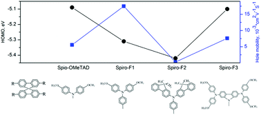
Spiro-F1 and Spiro-F3 exhibit deeper HOMO levels and higher hole mobilities than Spiro-OMeTAD, so they will emerge as potential HTM candidates for efficient PSC applications.
The content of this RSS Feed (c) The Royal Society of Chemistry