Nature Electronics, Published online: 12 August 2024; doi:10.1038/s41928-024-01219-8
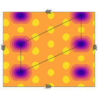
An antiferromagnetic diode effect was observed in a centrosymmetric crystal without directional charge separation. This effect could be used to create in-plane field-effect transistors and microwave-energy-harvesting devices.jinzhitong
Shared posts
13 Aug 01:08
An antiferromagnetic diode effect in even-layered MnBi2Te4
by Anyuan Gao
ytdcty likes this
13 Aug 01:08
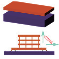
A scalable integration process for ultrafast two-dimensional flash memory
by Yongbo Jiang
Nature Electronics, Published online: 12 August 2024; doi:10.1038/s41928-024-01229-6
A scalable integration process for ultrafast two-dimensional flash memory can be used to integrate 1,024 devices with a yield of over 98%. The channel length of the devices could also be scaled down to sub-10 nm.
13 Aug 01:07
Circuit quantum electrodynamics detection of induced two-fold anisotropic pairing in a hybrid superconductor–ferromagnet bilayer
by C. G. L. Bøttcher
Nature Physics, Published online: 12 August 2024; doi:10.1038/s41567-024-02613-x
Heterostructures of ferromagnets and superconductors may host exotic superconducting states. Now a circuit quantum electrodynamics technique is demonstrated that provides evidence for triplet p-wave pairing in such a heterostructure.
13 Aug 01:01
Ultraflat single-crystal hexagonal boron nitride for wafer-scale integration of a 2D-compatible high-κ metal gate
by Yani Wang
Nature Materials, Published online: 12 August 2024; doi:10.1038/s41563-024-01968-z
The synthesis of wafer-scale ultraflat single-crystal hexagonal boron nitride film is realized by strong coupling to a Cu0.8Ni0.2(111)/sapphire wafer, providing a potential method for industry-compatible high-κ dielectric integration in two-dimensional electronics.
13 Aug 01:01
Two-dimensional electrons at mirror and twistronic twin boundaries in van der Waals ferroelectrics
by James G. McHugh
Nature Communications, Published online: 09 August 2024; doi:10.1038/s41467-024-51176-1
The authors investigate the twin boundaries in ferroelectric transition metal dichalcogenides, predicting their trap electrons with low densities, enhancing electron-electron interactions and potentially promoting Wigner crystallisation.
Alex Strasser, Sonny Rhim likes this
13 Aug 01:01
Electrical switching of spin-polarized light-emitting diodes based on a 2D CrI3/hBN/WSe2 heterostructure
by Jianchen Dang
Nature Communications, Published online: 09 August 2024; doi:10.1038/s41467-024-51287-9
Spin-polarized light-emitting diodes (spin-LEDs) convert the electronic spin information to photon circular polarization, but they are usually controlled only by external magnetic fields. Here, the authors report the realization of spin-LEDs based on 2D CrI3/hBN/WSe2 heterostructures, showing electrical tunability of the electroluminescence helicity.
Alex Strasser likes this
13 Aug 01:00
A clean transfer approach to prepare centimetre-scale black phosphorus crystalline multilayers on silicon substrates for field-effect transistors
by Yuqian Zhao
Nature Communications, Published online: 09 August 2024; doi:10.1038/s41467-024-51140-z
Black phosphorus (BP) is a 2D semiconductor with potential for (opto-)electronic applications, but its large-scale integration with Si substrates is challenging. Here, the authors report a method to transfer cm-scale BP films onto SiO2/Si substrates retaining their uniformity and electrical properties.
09 Aug 01:55
Collective Charge Excitations between Moiré Minibands in Twisted ${\mathrm{WSe}}_{2}$ Bilayers Probed with Resonant Inelastic Light Scattering
by Nihit Saigal, Lennart Klebl, Hendrik Lambers, Sina Bahmanyar, Veljko Antić, Dante M. Kennes, Tim O. Wehling, and Ursula Wurstbauer
Author(s): Nihit Saigal, Lennart Klebl, Hendrik Lambers, Sina Bahmanyar, Veljko Antić, Dante M. Kennes, Tim O. Wehling, and Ursula Wurstbauer
Collective electronic excitations between moiré-bands in twisted WSe2 bilayers may be probed by resonant inelastic light scattering, a sensitive way to access the moiré-bands and to study their unique properties.

[Phys. Rev. Lett. 133, 046902] Published Tue Jul 23, 2024
09 Aug 01:55
Hybrid van der Waals Epitaxy
by Lin Hu, Danshuo Liu, Fawei Zheng, Xuelin Yang, Yugui Yao, Bo Shen, and Bing Huang
Author(s): Lin Hu, Danshuo Liu, Fawei Zheng, Xuelin Yang, Yugui Yao, Bo Shen, and Bing Huang
The growth of a nitride epilayer on a van der Waals substrate follows a new growth mechanism, different from the previously known models of material growth.

[Phys. Rev. Lett. 133, 046102] Published Wed Jul 24, 2024
09 Aug 01:53
Separation of Inverse Altermagnetic Spin-Splitting Effect from Inverse Spin Hall Effect in ${\mathrm{RuO}}_{2}$
by Ching-Te Liao, Yu-Chun Wang, Yu-Cheng Tien, Ssu-Yen Huang, and Danru Qu
Author(s): Ching-Te Liao, Yu-Chun Wang, Yu-Cheng Tien, Ssu-Yen Huang, and Danru Qu
By isolating the relativistic spin Hall effect in an epitaxially grown film of RuO2 with well-defined Néel vectors, the spin-to-charge conversion of the nonrelativistic altermagnetic spin-splitting has been demonstrated.

[Phys. Rev. Lett. 133, 056701] Published Tue Jul 30, 2024
09 Aug 01:53
Prevalence of Two-Dimensional Photonic Topology
by Ali Ghorashi, Sachin Vaidya, Mikael C. Rechtsman, Wladimir A. Benalcazar, Marin Soljačić, and Thomas Christensen
Author(s): Ali Ghorashi, Sachin Vaidya, Mikael C. Rechtsman, Wladimir A. Benalcazar, Marin Soljačić, and Thomas Christensen
Despite intense research in topological photonics for more than a decade, the basic question of whether photonic band topology is rare or abundant—i.e., its relative prevalence—remains open. Here, we use symmetry analysis and a dataset of 550 000 synthetic two-dimensional photonic crystals to determ…
[Phys. Rev. Lett. 133, 056602] Published Fri Aug 02, 2024
09 Aug 01:53
Interaction-Driven Quasi-Insulating Ground States of Gapped Electron-Doped Bilayer Graphene
by Anna M. Seiler, Martin Statz, Isabell Weimer, Nils Jacobsen, Kenji Watanabe, Takashi Taniguchi, Zhiyu Dong, Leonid S. Levitov, and R. Thomas Weitz
Author(s): Anna M. Seiler, Martin Statz, Isabell Weimer, Nils Jacobsen, Kenji Watanabe, Takashi Taniguchi, Zhiyu Dong, Leonid S. Levitov, and R. Thomas Weitz
Bernal bilayer graphene has recently been discovered to exhibit a wide range of unique ordered phases resulting from interaction-driven effects and encompassing spin and valley magnetism, correlated insulators, correlated metals, and superconductivity. This Letter reports on a novel family of correl…
[Phys. Rev. Lett. 133, 066301] Published Mon Aug 05, 2024
09 Aug 01:53
Dispersion-Selective Band Engineering in an Artificial Kagome Superlattice
by Shuai Wang, Zhen Zhan, Xiaodong Fan, Yonggang Li, Pierre A. Pantaleón, Chaochao Ye, Zhiping He, Laiming Wei, Lin Li, Francisco Guinea, Shengjun Yuan, and Changgan Zeng
Author(s): Shuai Wang, Zhen Zhan, Xiaodong Fan, Yonggang Li, Pierre A. Pantaleón, Chaochao Ye, Zhiping He, Laiming Wei, Lin Li, Francisco Guinea, Shengjun Yuan, and Changgan Zeng
Researchers have used a specially crafted electric potential to manipulate the electronic band structure of graphene, laying the groundwork for on-demand electronic band design.

[Phys. Rev. Lett. 133, 066302] Published Tue Aug 06, 2024
09 Aug 01:52
Quantum Anomalous Hall Crystal at Fractional Filling of Moiré Superlattices
by D. N. Sheng, Aidan P. Reddy, Ahmed Abouelkomsan, Emil J. Bergholtz, and Liang Fu
Author(s): D. N. Sheng, Aidan P. Reddy, Ahmed Abouelkomsan, Emil J. Bergholtz, and Liang Fu
States called quantum anomalous Hall crystals exhibit a quantized Hall conductance with a larger than expected value.

[Phys. Rev. Lett. 133, 066601] Published Wed Aug 07, 2024
09 Aug 01:52
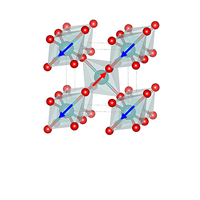
Origin of a Topotactic Reduction Effect for Superconductivity in Infinite-Layer Nickelates
by Shengwei Zeng, Chi Sin Tang, Zhaoyang Luo, Lin Er Chow, Zhi Shiuh Lim, Saurav Prakash, Ping Yang, Caozheng Diao, Xiaojiang Yu, Zhenxiang Xing, Rong Ji, Xinmao Yin, Changjian Li, X. Renshaw Wang, Qian He, Mark B. H. Breese, A. Ariando, and Huajun Liu
Author(s): Shengwei Zeng, Chi Sin Tang, Zhaoyang Luo, Lin Er Chow, Zhi Shiuh Lim, Saurav Prakash, Ping Yang, Caozheng Diao, Xiaojiang Yu, Zhenxiang Xing, Rong Ji, Xinmao Yin, Changjian Li, X. Renshaw Wang, Qian He, Mark B. H. Breese, A. Ariando, and Huajun Liu
Spectroscopic and transport measurements on optimally reduced nickelate films show a single dx2−y2 orbital occupancy leading to the minimization of the c-axis parameter, a correlation between the orbital asymmetry and the Tc which supports the electronic analogy between nickelate and cuprate superconductors.

[Phys. Rev. Lett. 133, 066503] Published Thu Aug 08, 2024
09 Aug 01:48
2D transistors feel the squeeze
by Stuart Thomas
Nature Electronics, Published online: 24 July 2024; doi:10.1038/s41928-024-01225-w
2D transistors feel the squeeze
09 Aug 01:48
Critical challenges in the development of electronics based on two-dimensional transition metal dichalcogenides
by Yan Wang
Nature Electronics, Published online: 29 July 2024; doi:10.1038/s41928-024-01210-3
This Perspective explores key challenges in the development of electronics based on two-dimensional transition metal dichalcogenides, identifying defects, doping, p-type contacts and high-dielectric-constant dielectrics as critical issues.
09 Aug 01:45
A leap to highly efficient 2D quantum emitters
by Su-Hyun Gong
Nature Photonics, Published online: 05 August 2024; doi:10.1038/s41566-024-01487-y
A plasmonic platform and a dual gate are integrated in a single-photon emitter made of two-dimensional materials. The combination enables engineered radiative and nonradiative decays, leading to a device quantum efficiency of up to 90%.
Alex Strasser likes this
09 Aug 01:44
Colossal in-plane optical anisotropy in a two-dimensional van der Waals crystal
by Qiangbing Guo
Nature Photonics, Published online: 08 August 2024; doi:10.1038/s41566-024-01501-3
A two-dimensional van der Waals material, NbOCl2, that simultaneously exhibits near-unity linear dichroism (~99%) over 100 nm bandwidth in ultraviolet regime and large birefringence (0.26–0.46) within a wide visible–near-infrared transparency window is reported.
Alex Strasser likes this
09 Aug 01:41
Monolithic three-dimensional integration of complementary two-dimensional field-effect transistors
by Rahul Pendurthi
Nature Nanotechnology, Published online: 23 July 2024; doi:10.1038/s41565-024-01705-2
Monolithic 3D integration of complementary WSe2 FETs has been achieved, featuring n-type FETs in tier 1 and p-type FETs in tier 2. Dense vias are realized using a pitch of less than 1 µm, facilitating 3D inverters as well as NAND and NOR logic functionalities.
jinzhitong likes this
09 Aug 01:41
Charge-transfer contacts for the measurement of correlated states in high-mobility WSe2
by Jordan Pack
Nature Nanotechnology, Published online: 25 July 2024; doi:10.1038/s41565-024-01702-5
By utilizing the van der Waals electron acceptor α-RuCl3, this study establishes a p-type connection with WSe2, facilitating a high hole mobility of 80,000 cm2 V–1 s–1 for investigating quantum transport properties in a magnetic field of over 30 T.
09 Aug 01:40
Doping a frustrated correlated van der Waals magnet
by Jose L. Lado
Nature Materials, Published online: 01 August 2024; doi:10.1038/s41563-024-01948-3
When many-body correlations in quantum materials control the motion of electrons, new quantum states can emerge. Now, a study demonstrates that doping a van der Waals correlated insulator leads to collective electronic reordering arising due to quantum many-body interactions.
09 Aug 01:40
Seeing ferroelectric phase transitions
by Ignasi Fina
Nature Materials, Published online: 01 August 2024; doi:10.1038/s41563-024-01930-z
Real-time atomic-scale imaging reveals the presence of reversible transitions between ferroelectric and non-ferroelectric phases during electric stimuli, enabling the possibility for reliability improvement in ferroelectric materials compatible with complementary metal–oxide–semiconductors.
09 Aug 01:39
Tunable even- and odd-denominator fractional quantum Hall states in trilayer graphene
by Yiwei Chen
Nature Communications, Published online: 24 July 2024; doi:10.1038/s41467-024-50589-2
The fractional quantum Hall effect offers a potential platform to harness non-Abelian anyons. Here, the authors report fractional quantum Hall states in trilayer graphene and drive quantum phase transitions between neighbouring states.
Alex Strasser likes this
09 Aug 01:37
Alkali cation stabilization of defects in 2D MXenes at ambient and elevated temperatures
by Brian C. Wyatt
Nature Communications, Published online: 28 July 2024; doi:10.1038/s41467-024-50713-2
The effect of defects on MXene structural transitions in high-temperature environments is shown. Further, defect occupied alkali cations are shown to improve MXenes’ phase stability and control surface diffusion related phase changes.
09 Aug 01:37
Author Correction: From bulk effective mass to 2D carrier mobility accurate prediction via adversarial transfer learning
by Xinyu Chen
Nature Communications, Published online: 31 July 2024; doi:10.1038/s41467-024-50561-0
Author Correction: From bulk effective mass to 2D carrier mobility accurate prediction via adversarial transfer learning
09 Aug 01:36
Evidence of electron interaction with an unidentified bosonic mode in superconductor CsCa2Fe4As4F2
by Peng Li
Nature Communications, Published online: 31 July 2024; doi:10.1038/s41467-024-50833-9
The kink structure in the band dispersion can be linked to electron-boson interaction and has been reported in unconventional superconductors. Here the authors observe an orbital selective and momentum dependent kink feature in an Fe-based superconductor, which is highly correlated with superconductivity.
09 Aug 01:35
Ag2Se as a tougher alternative to n-type Bi2Te3 thermoelectrics
by Min Liu
Nature Communications, Published online: 03 August 2024; doi:10.1038/s41467-024-50898-6
The authors report better toughness in n-type Ag2Se than commercial Bi2Te3. The fabricated n-Ag2Se/p-Bi2Te3 modules show good performance and long-term stability for both refrigeration and power generation near room temperature.
ChenDH, Sonny Rhim likes this
09 Aug 01:34
Controlled interlayer exciton ionization in an electrostatic trap in atomically thin heterostructures
by Andrew Y. Joe
Nature Communications, Published online: 08 August 2024; doi:10.1038/s41467-024-51128-9
Here, the authors use electrostatic gates to trap interlayer excitons (IE) in MoSe2/WSe2 heterobilayers. They observe an exponential broadening of the IE emission linewidth that signals the IE ionization threshold.
09 Aug 01:29
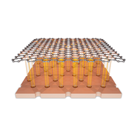
Single-crystalline metal-oxide dielectrics for top-gate 2D transistors
by Daobing Zeng
Nature, Published online: 07 August 2024; doi:10.1038/s41586-024-07786-2
By using intercalative oxidation techniques, stable, stoichiometric and atomically thin single-crystalline Al2O3 films can be produced, which can be effectively used as a dielectric in top-gated field-effect transistors based on two-dimensional materials.