Hot off AMD’s Capsaicin GDC 2016 event, the company has just unveiled Vega & Navi its next generation post Polaris Radeon graphics architectures. Coming in 2017 and 2018 Respectively. Featuring HBM2 vertically stacked memory technology. nextgen post-HBM2 memory and very significant power efficiency jumps every year.

AMD’s Raja Koduri, head of Radeon Technologies Group, just revealed the company’s future GPU architectures all of which will be named after stars, star systems and galaxies. The company’s head of the newly founded Radeon Technologies Group explained that the team is heading towards a new direction with a fresh look on all things graphics and there was a need to reflect this change of winds.
AMD Radeon Technologies Group Bids A Somber Farewell To Island Code Names And Begins Its “Journey Into Space”
One of the most exciting things about AMD’s next generation Polaris graphics architecture is the highly anticipated move to the revolutionary FinFET process technology. Which is accompanied by a considerable engineering focus to push innovations on architectural efficiency.
AMD has consistently said that the Polaris graphics architecture will deliver a “historic” leap in performance per watt. This unprecedented improvement in performance per watt is where the naming convention stems from. This is because stars are the most efficient photon generators in the universe,. Which explains why folks at AMD found it only fitting to call their most power efficient graphics architecture to date “Polaris” after the brightest star that can be seen from earth’s surface.

Excerpt from AMD’s Official Polaris Press Release :
AMD’s Polaris architecture-based 14nm FinFET GPUs deliver a remarkable generational jump in power efficiency. Polaris-based GPUs are designed for fluid frame rates in graphics, gaming, VR and multimedia applications running on compelling small form-factor thin and light computer designs.
“Our new Polaris architecture showcases significant advances in performance, power efficiency and features,” said Lisa Su, president and CEO, AMD. “2016 will be a very exciting year for Radeon fans driven by our Polaris architecture, Radeon Software Crimson Edition and a host of other innovations in the pipeline from our Radeon Technologies Group.”
Raja Koduri, vice president at AMD and chief architect of the Radeon Technologies Group explained before that he holds a very ambitious goal of powering 90% of the world’s pixels. To achieve that efficiency goal is key and just as stars are the world’s most efficient photon generators, Koduri wants AMD graphics technology to be the world’s most efficient pixel generators.
One of the more notable changes that the Radeon Technologies Group is doing is giving its next gen graphics architectures unifying code names. Something the company hasn’t done consistently in the past, not in any official capacity anyway. Raja explained earlier in the year that this change will make things easier for everyone involved. Whether it be internally at AMD, journalists or even consumers. Raja confirmed that of AMD’s future graphics architectures will be given astronomical code names. Polaris being the first that will begin Radeon Technologies Group’s re-invigorated journey into space.
Raja Koduri, Senior Vice President and Chief Architect, Radeon Technologies Group, speaking with Venturebeat.com :
We have some exciting hardware announcements as well. This is designed for FinFET. Our guiding principle for the Polaris architecture was power efficiency. We have the new naming scheme for our architectures. It’ll be based on galaxies, star systems, and stars. You’ll see more of this coming in the future. Polaris is the beginning of our journey through space.
VB: Does the Polaris brand supplant the Radeon brand?
Koduri: It’s an architecture codename. It’ll still be Radeon something something on the box. But we didn’t have a consistent architecture name like our competitors do. It was hard, because for people, including yourselves and some of the press and enthusiasts—This family of chips has this architecture and a similar class of features. You can group them easily together.
[Exclusive] AMD’s Greenland Has Been Known As “Vega 10” Internally For Some Time
Two months ago we published an exclusive story explaining what Vega 10 was and what had happened to AMD’s flagship Greenland GPU. Today at Capsiacin – GDC 2016 – AMD has confirmed exactly what we had conveyed to you in that report.
Vega is the brightest star in the Lyra constellation and the second brightest star in the northern hemisphere. Vega along with Arcturus and Sirius, is one of the most luminous stars close to our earth’s own sun. Vega has been extensively studied by astronomers and as such was described as “arguably the next most important star in the sky after the Sun”. Furthermore, it was the northern pole star around 12,000 BCE.
Vega was the first star other than the Sun to be photographed and the first to have its spectrum recorded. But perhaps the most significant fact of all about Vega is that it served as the baseline for calibrating the photometric brightness scale, and was one of the stars used to define the mean values for the UBV photometric system.
This preface is important in underlining why the Vega code name bears a special meaning for AMD and why AMD has chosen to dedicate it to its most power 14nm GPU to date. Greenland / Vega 10 will be the first GPU from the company to feature HBM2 – High Bandwidth Memory – Technology. All of this is part of AMD’s strategy to deploy this extremely power efficient and innovative memory standard in its high-end graphics products first and eventually into mainstream GPUs and even APUs.
AMD To Introduce Vega With HBM2 in 2017
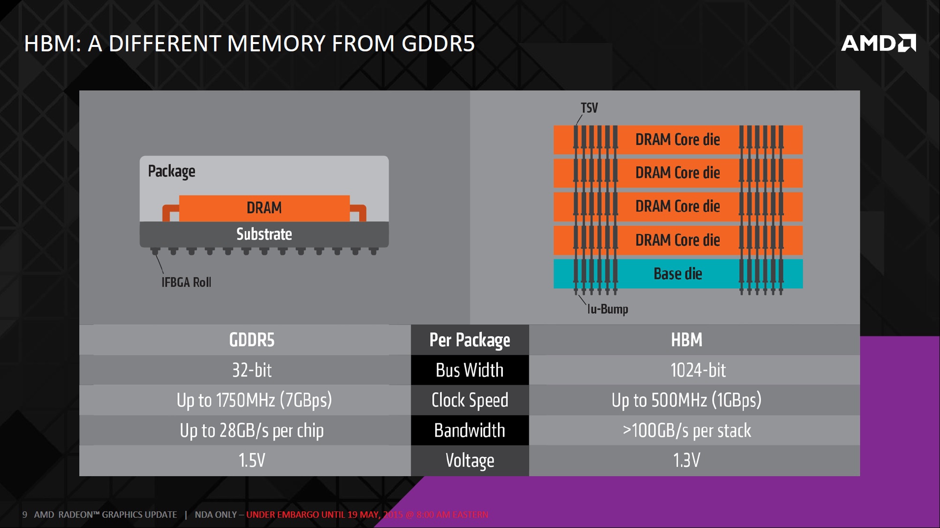
The Fiji GPU powering the R9 Fury series is AMD’s largest ever graphics processing unit. It’s also the world’s only and first to feature the 3D structured, 2.5D stacked High Bandwidth Memory, . This standard was co-invented by AMD and SK Hynix, one of the world’s largest memory makers. The advantages of vertically stacking dies are many. One of which is the enablement of significantly greater densities versus GDDR5. Also because HBM cubes occupy a lot less space than GDDR5 engineers can achieve tremendous area savings on the printed circuit board of any HBM graphics card. This allowed for the creation of world’s fastest SFF six inch graphics card, the 8 teraflops R9 Nano.
There are also other innovations that HBM leverages. One of which is packaging. Because it sits next to the GPU on an interposer, a very short distance away, it allows engineers to create immensely wider memory busses with reduced latency and very low power requirements. The end result translates to a memory standard that’s very power efficient, very area efficient and very scalable and very fast.
Earlier this year AMD confirmed to us that while it is still committed to the High Bandwidth Memory technology it co-invented with SK Hynix and brought to the market last year, Polaris was designed to be compatible with both HBM/HBM2 and GDDR5 memory standards. Technical marketing lead at AMD Robert Hallock explained that the company has the flexibility to use either technology as needs arise. This means that either memory technology can be employed where it makes sense.
AMD helped lead the development of HBM, was the first to bring HBM to market in GPUs, and plans to implement HBM/HBM2 in future graphics solutions.
At this time we have only publicly demonstrated a GDDR5 configuration of the Polaris architecture.It’s important to understand that HBM isn’t (currently) suitable for all GPU segments due to the current HBM cost structure. In the mainstream GPU segment, GDDR5 remains an extremely cost-effective, efficient and viable memory technology.
It’s now clear that AMD’s plan is to introduce HBM2 technology with it’s upcoming Vega graphics architecture, which will be launching next year. HBM2 is the second generation of the vertically stacked High Bandwidth Memory standard that AMD introduced last year with its flagship Radeon R9 Fury X graphics card, the R9 Fury and the R9 Nano.

Second generation High Bandwidth Memory is not only faster than the first generation but it also scales to capacities 8 times larger than HBM1. HBM2 feature 1GB per die and up to 8 Hi stacks for 8GB per cube. Which is eight times more than the highest capacity currently available per cube on HBM1. Additionally, HBM2 operates at twice the speed of HBM1 for double the memory bandwidth.
This means that AMD can equip its flagship Vega 10 GPU with up to 32GB of super high speed HBM2 memory for a total of terabyte/s of memory bandwidth. However we’ll have to wait until 2017 for the 14nm process technology and the HBM2 technology to mature enough for such a monstrous chip. Polaris graphics cards on the other hand are coming out this summer, before the back to school season, on both desktops and gaming notebooks.
| WCCFTech |
Year |
Process |
Flagship GPU |
Product |
Transistors In Billions |
Memory |
Bandwidth |
| Southern Islands |
2012 |
28nm |
Tahiti |
HD 7970 |
4.3 |
3GB GDDR5 |
264GB/s |
| Volcanic Islands |
2013 |
28nm |
Hawaii |
R9 290X |
6.2 |
4GB GDDR5 |
320GB/s |
| Pirate/Caribbean Islands |
2015 |
28nm |
Fiji |
R9 Fury X |
8.9 |
4GB HBM1 |
512GB/s |
| Arctic Islands/Polaris |
2016 |
14nm |
Polaris |
TBA |
Up To 18 |
GDDR5/HBM1 |
512 GB/s |
| Next Gen GPU Family |
2017 |
14nm |
Vega |
TBA |
TBA |
HBM2 |
1 TB/s |
| Next Gen GPU Family |
2018 |
TBA |
Navi |
TBA |
TBA |
Nextgen Memory |
TBA |
Note: There is a poll embedded within this post, please visit the site to participate in this post's poll.
The post AMD Unveils Vega & Navi, 2017 & 18 Graphics Architectures – To Bring HBM2 & Nextgen Memory To Market by Khalid Moammer appeared first on WCCFtech.


